
By João Silva
Graphics Component Analysis
Intel’s architectural roadmap appears to be undergoing a significant, if somewhat surprising, recalibration. New industry reports suggest that the silicon giant is developing a high-performance APU project codenamed "Razor Lake-AX." This development marks a dramatic reversal of the company’s previous stance on on-package memory, signaling that Intel is once again prioritizing architectural density and bandwidth to compete in the burgeoning "Halo-class" processor market.
Main Facts: The Return of On-Package Memory
The most striking aspect of the Razor Lake-AX rumors is the reported return of on-package memory (OPM). Previously, Intel executives had framed the memory-on-package design—first debuted in the Lunar Lake (Core Ultra 200V) series—as a "one-off" experiment. The rationale provided at the time centered on the immense cost, supply chain complexity, and the potential for reduced repairability and flexibility in the OEM market.
However, according to industry insiders such as Jaykihn and Haze, the engineering requirements for Razor Lake-AX necessitate this technology’s return. The processor is expected to leverage high-speed memory, likely LPDDR5X, integrated directly onto the package. This design choice is not merely an aesthetic or space-saving measure; it is a technical imperative. By situating the memory in such close proximity to the processor, Intel aims to slash latency and maximize memory throughput—bottlenecks that have historically hampered the performance of integrated graphics in traditional architectures.
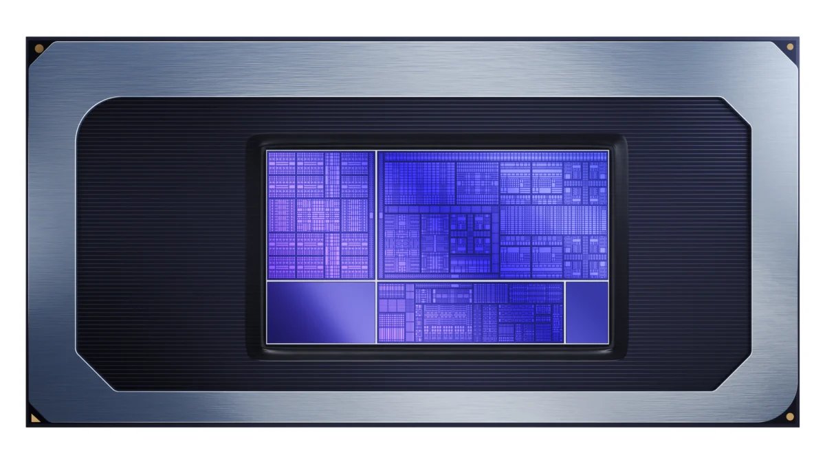
Beyond the memory architecture, the GPU configuration is set to be a significant leap forward. Reports indicate that Razor Lake-AX will feature either 16 or 32 Xe3 graphics cores. While this count sits below the previously rumored 48-core Xe setup associated with the defunct Nova Lake-AX project, 32 cores represent a formidable amount of compute power for an integrated solution.
Chronology of Development: From Lunar Lake to Razor Lake
To understand the significance of Razor Lake-AX, one must trace the recent trajectory of Intel’s client computing division:
- Late 2024 (Lunar Lake Launch): Intel introduced the Core Ultra 200V series, featuring "Memory-on-Package." It was marketed as a breakthrough in mobile power efficiency and footprint reduction.
- Early 2025: Internal discussions regarding "Nova Lake-AX" surfaced, suggesting an ambitious project with 48 Xe-core integrated graphics.
- Mid-2025: Intel publicly walked back the expectation of on-package memory becoming a standard, citing the "margin complexities" of the Lunar Lake design.
- Late 2025/Early 2026: Nova Lake-AX faced uncertainty as Intel’s roadmap saw adjustments to reflect shifting market demands and foundry capacities.
- Present (2026): Leaks regarding "Razor Lake-AX" indicate that the core principles of the Lunar Lake design (OPM) have been revived, not as a mainstream consumer standard, but as a specialized, high-performance tool intended to challenge market leaders in the "Halo" APU segment.
Supporting Data: Why 32 Xe3 Cores Matter
The jump to 32 Xe3 cores in a monolithic or chiplet-based APU is not trivial. In the current landscape, integrated graphics are often starved of bandwidth. Traditional SODIMM or soldered LPDDR5 configurations outside of the package are limited by the physical distance between the RAM and the GPU, as well as the overhead of the memory controller bus.

By integrating the memory directly onto the package, Intel is essentially creating a high-speed "buffer" that allows the Xe3 graphics engine to operate at its full potential. A 32-core Xe3 configuration, if properly fed with data, could theoretically outperform many entry-level discrete GPUs currently found in thin-and-light laptops.
Furthermore, the utilization of the BGA4326 socket confirms that Razor Lake-AX is not aimed at the DIY desktop market. Instead, this is a premium silicon solution designed for high-end workstations, SFF (Small Form Factor) powerhouses, and potentially, the high-performance handheld gaming segment. This socket size suggests a massive, feature-dense package, likely combining high-performance P-cores with a dense array of E-cores, alongside the massive iGPU.
Official Responses and Industry Context
Intel has remained characteristically tight-lipped regarding "Razor Lake-AX," as is standard for unreleased, multi-year projects. However, the company has consistently emphasized its "IDM 2.0" strategy, which involves utilizing its own advanced packaging technologies (such as Foveros) to integrate disparate silicon dies.
The industry response, however, has been speculative and intense. Analysts point out that Intel is currently in a "pincer movement" between two distinct competitors:
- AMD: The "Strix Halo" and "Medusa" APU architectures are already pushing the boundaries of what consumers expect from an APU. AMD has leveraged its chiplet expertise to pack substantial GPU power into a mobile-friendly package.
- Apple: The M-Series Pro and Max silicon remains the gold standard for unified memory architecture (UMA) performance. Apple’s ability to optimize hardware and software through its custom memory controllers has forced the rest of the industry—Intel included—to rethink how they handle memory latency.
Intel’s shift to Razor Lake-AX is a clear response to these pressures. They are no longer content to let AMD and Apple dominate the high-performance integrated graphics space. By reviving the "one-off" memory strategy, they are admitting that to compete with the M4/M5 Pro/Max series, the traditional "CPU-plus-external-RAM" model is no longer sufficient.
Implications: The Future of "Halo" APUs
The emergence of Razor Lake-AX suggests that we are entering a new era of "Halo APUs"—processors that effectively render entry-level discrete graphics cards redundant.
Performance Implications
If Intel successfully executes the Razor Lake-AX design, the primary beneficiaries will be creative professionals and power-users who require high GPU compute in a portable form factor. The integration of 32 Xe3 cores suggests that video editing, 3D rendering, and AI-accelerated workflows could see significant boosts in efficiency, as data no longer needs to traverse the motherboard traces to reach the GPU.

Market Implications
For the consumer, this will likely lead to a bifurcation of the laptop market. On one end, we will have thin, efficient "Razor-class" machines that offer professional-grade performance without the need for a dedicated, power-hungry GPU. On the other, we will have traditional gaming laptops that continue to rely on desktop-class discrete GPUs.
However, the cost remains a significant barrier. On-package memory increases the manufacturing complexity of the CPU package exponentially. If a single memory chip on the package fails, the entire processor becomes a write-off. This suggests that Razor Lake-AX will be an incredibly expensive piece of silicon, likely reserved for the $2,000+ laptop segment.
Competitive Outlook
The race to 2027 is now set. AMD’s Medusa architecture and Apple’s next-generation silicon will be the benchmarks against which Razor Lake-AX is measured. For Intel, this project is a "must-win." The company needs to prove that it can maintain its lead in CPU instruction-per-clock performance while simultaneously delivering a graphics engine that is not just competitive, but revolutionary.
Conclusion: A Gamble on Complexity
Intel’s "Razor Lake-AX" is a fascinating example of how market pressures can force a company to abandon its own strategic guidelines. What was once deemed a "one-off" experiment with Lunar Lake has now become the blueprint for Intel’s most ambitious APU project to date.
By prioritizing bandwidth via on-package memory and pushing the Xe3 architecture to its physical limits, Intel is signaling a return to the "performance at any cost" philosophy. Whether or not this strategy will allow them to reclaim the throne from AMD and Apple remains to be seen, but one thing is clear: the next two years of processor development will be defined by the battle for the "Halo" segment, and Razor Lake-AX is Intel’s heaviest weapon in that fight.
Disclaimer: The information provided in this article is based on industry reports and leaks. Official specifications and release dates are subject to change by Intel as the product moves through the validation phase.