
 Pevita Pearce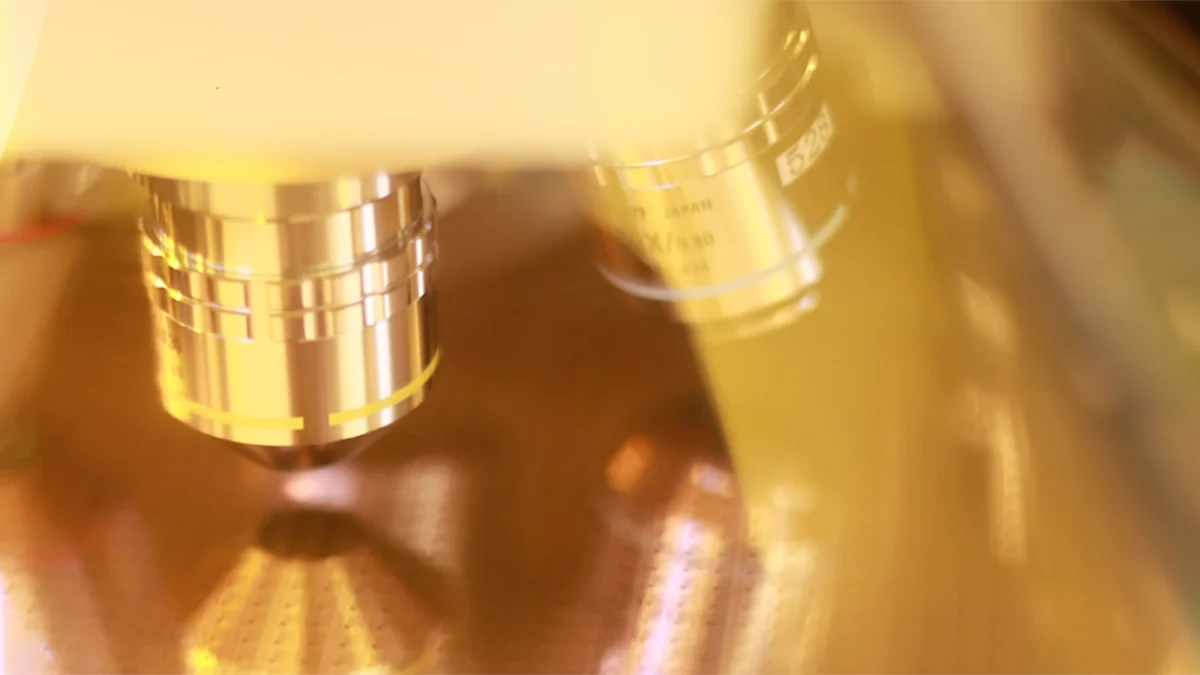
The global semiconductor landscape stands at a precarious juncture as China accelerates its quest for technological self-reliance. Following recent reports confirming that China has begun mass-producing domestic immersion deep ultraviolet (DUV) lithography machines—a critical piece of hardware required to manufacture advanced logic and memory chips—the identity of the lead manufacturer has finally surfaced.
According to a recent report by Reuters, the state-backed entity spearheading this monumental industrial effort is Shanghai Aishengna Electronic Technology Group. This revelation provides a missing piece of the puzzle in the narrative of China’s "Big Fund" initiatives, which seek to circumvent tightening international export controls on high-end chipmaking equipment.
The Genesis of Shanghai Aishengna Electronic Technology Group
Established in August 2023 with a staggering registered capital of RMB 7 billion (approximately $1 billion USD), Shanghai Aishengna Electronic Technology Group was engineered to serve as the nucleus for China’s advanced lithography ambitions. Its formation represents a strategic consolidation of talent and resources rather than a greenfield startup.
Industry analysts suggest that Aishengna has effectively absorbed elite engineering teams from two pivotal, albeit previously fragmented, players in the domestic ecosystem: Shanghai Yuliangsheng Technology and Shanghai Micro Electronics Equipment (SMEE). By centralizing these assets, the state-backed firm aims to streamline the complex research and development cycles inherent in DUV technology, which has historically been dominated by the Dutch giant ASML.
Chronology of the Domestic Lithography Push
The journey toward domestic immersion DUV capability has been characterized by years of intense, state-sponsored R&D, punctuated by rapid acceleration in the last 24 months.
- Pre-2023: China relies heavily on imports for immersion DUV scanners. Restrictions imposed by the United States and its allies on the export of advanced lithography tools to China create a significant "technology ceiling," capping China’s ability to produce chips below 7nm nodes at scale.
- August 2023: Shanghai Aishengna Electronic Technology Group is officially incorporated. With $1 billion in capital, the company is positioned as the primary vehicle for high-end lithography manufacturing.
- Late 2023–Early 2025: Intense integration efforts take place. Engineering teams from SMEE and Yuliangsheng are consolidated under the Aishengna banner to focus on the technical hurdles of immersion optics and precision stages.
- September 2025: Semiconductor Manufacturing International Corporation (SMIC), China’s largest foundry, begins active testing of an immersion lithography tool developed under the Yuliangsheng/Aishengna pipeline. This represents the first major real-world trial of domestic equipment in a production-grade environment.
- Late 2025/Early 2026: Reports confirm the commencement of mass production for domestic immersion DUV scanners, signaling a shift from laboratory prototypes to commercial deployment.
Supporting Data and Technical Context
Immersion DUV lithography is the backbone of modern chip fabrication. Unlike dry lithography, immersion technology uses a liquid medium (typically ultrapure water) between the lens and the silicon wafer to increase the numerical aperture (NA) of the optical system. This allows for the printing of smaller, more intricate circuit patterns.
The significance of Aishengna’s progress cannot be overstated. By successfully domesticating this technology, China aims to secure its supply chain for several major industry players:
- SMIC: The primary beneficiary, currently attempting to scale its 7nm and 5nm-class production lines without reliance on restricted foreign machinery.
- Hua Hong Semiconductor: A key player in specialty technologies, now poised to upgrade its node capabilities.
- ChangXin Memory Technologies (CXMT): China’s leading DRAM manufacturer, which requires DUV scanners to maintain competitiveness in the global memory market.
The RMB 7 billion investment is only the tip of the iceberg. Behind this capital injection lies a massive supply chain of sub-component manufacturers providing high-precision laser sources, optical coatings, and vibration-dampening stages—all of which have been under heavy pressure to reach international standards.
Silence from Stakeholders: The Policy of Ambiguity
The disclosure of Aishengna as the manufacturer remains, for the moment, an attribution by a single anonymous source close to the project. Despite the specificity of the report, official channels remain remarkably quiet.
Both SMEE and Yuliangsheng have declined to respond to repeated requests for comment. This silence is consistent with the standard operating procedure for China’s high-tech sector, where projects of strategic national importance are frequently shrouded in layers of non-disclosure agreements and state-secret protocols. For the Chinese government, maintaining ambiguity serves two purposes: it shields the company from further targeted international sanctions and protects the proprietary nature of the breakthroughs achieved in the "trial-and-error" phase of development.
Furthermore, industry experts note that the lack of public statements from SMIC regarding the performance of the domestic tool is indicative of the "burn-in" period. Until the equipment reaches a yield rate comparable to foreign competitors, the stakeholders are unlikely to make definitive claims.
Implications for Global Semiconductor Hegemony
The emergence of a domestic immersion DUV capability carries profound geopolitical and economic implications.
1. The Erosion of Export Control Efficacy
The core objective of US-led export restrictions was to slow the progression of the Chinese semiconductor industry by denying access to the machines that define the cutting edge. If Aishengna can successfully produce and maintain these machines, the "chokepoint" strategy effectively loses its teeth. While these domestic machines may lag behind the latest ASML scanners in terms of throughput (wafers per hour) and overlay precision, they provide an "indigenous alternative" that allows Chinese fabs to keep operating even in a total isolation scenario.
2. Supply Chain Bifurcation
The world is witnessing a clear bifurcation of the semiconductor supply chain. One path remains integrated with Western toolmakers, while the other is increasingly self-contained within the Chinese ecosystem. This creates a dual-standard industry where Chinese firms may soon operate on a distinct technological stack, potentially leading to a divergence in design standards and equipment interfaces.
3. Economic Pressure on Traditional Suppliers
While domestic tools may not immediately threaten the dominance of ASML or Japanese firms like Nikon and Canon, the "Made in China" mandate will inevitably eat into the market share of these companies within the Chinese market. As China accounts for a significant portion of global chipmaking equipment demand, a transition to domestic machinery could lead to a structural reduction in global revenue for established lithography giants.
4. The "Yield" Hurdle
Despite the breakthrough in production, the road ahead is fraught with challenges. Lithography is not just about the machine; it is about the "ecosystem of precision." Achieving mass production is one milestone, but reaching high-volume manufacturing (HVM) yields—where the vast majority of chips on a wafer are functional—is an entirely different hurdle. If Aishengna’s scanners suffer from high maintenance requirements or low reliability, the cost-per-chip for SMIC and others will remain unsustainably high.
Conclusion
The naming of Shanghai Aishengna Electronic Technology Group provides a face to the collective ambition of the Chinese state to master the most complex machine ever built. While the world watches to see if these machines can truly bridge the gap between laboratory success and factory-floor dominance, the development marks a definitive end to the era of total reliance on imported DUV technology.
As the first deliveries reach SMIC, Hua Hong, and CXMT, the global semiconductor industry enters a new, more volatile phase. The "Great Tech Decoupling" is no longer a theoretical projection; it is being etched, layer by layer, onto silicon wafers in the heart of Shanghai. Whether this domestic push will ultimately foster a new era of innovation or result in a high-cost, state-subsidized silo remains to be seen, but the intent—and the machinery—is now firmly in place.

 Nana Wu
 Ammar Sabilarrohman