
In the relentless pursuit of Moore’s Law, the semiconductor industry has shifted its focus from shrinking transistors to building upward. As we approach the physical limits of 2D scaling, 3D chip stacking has emerged as the primary vehicle for performance density. At the heart of this transition is hybrid bonding, a sophisticated copper-to-copper interconnection technique that effectively renders traditional solder microbumps obsolete.
While hybrid bonding has successfully revolutionized logic-to-logic and logic-to-cache integration, its adoption in the memory sector has hit a strategic speed bump. A recent decision by JEDEC—the global leader in developing open standards for the microelectronics industry—has effectively delayed the arrival of hybrid bonding in High Bandwidth Memory (HBM), setting the stage for a bifurcated evolution in chip architecture.
The Mechanics of the Hybrid Bond
To understand why the industry is so fixated on hybrid bonding, one must first understand the limitations of the status quo. Conventional 2.5D and 3D stacking rely on microbumps—tiny spheres of solder that act as electrical bridges between chips. As interconnect density requirements climb, these bumps become a bottleneck; they are bulky, prone to thermal fatigue, and inherently limited in their pitch (the distance between center points of connections).
Hybrid bonding removes the bump entirely. The process involves polishing the surface of two dies to an atomic level of flatness. Once the copper pads and their surrounding dielectric layers are aligned, they are bonded directly under intense heat and pressure. Because there is no solder to "collapse" or deform, engineers can pack these connections at significantly tighter pitches.
The density gains are staggering. Industry data, including metrics cited by AMD, suggests that hybrid bonding provides roughly 15 times the interconnect density of conventional microbump-based 3D stacking. TSMC’s recent technical symposiums have highlighted the disparity: while traditional face-to-back Through-Silicon-Via (TSV) stacking typically manages around 1,500 signals per square millimeter, face-to-face hybrid bonding can facilitate approximately 14,000 signals in the same area. This increase is the lifeblood of high-performance computing (HPC) and artificial intelligence, where memory-to-logic bandwidth is the ultimate performance limiter.
Chronology of an Industry Pivot
The trajectory of hybrid bonding has been marked by rapid adoption in the logic sector, contrasting sharply with the conservative, standard-driven nature of the memory market.
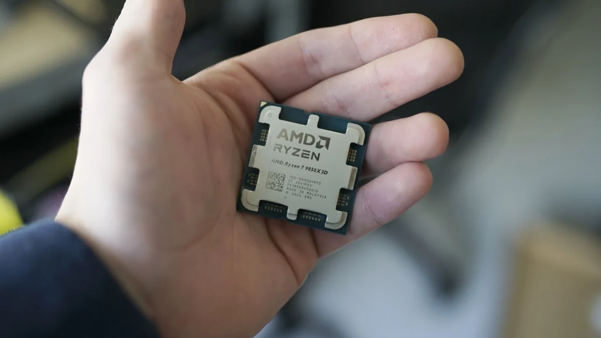
- 2020–2022: The Logic Breakthrough: AMD pioneered the commercial use of 3D hybrid bonding with its V-Cache technology. By stacking SRAM directly onto the processor die, AMD proved that the thermal and mechanical challenges of copper-to-copper bonding could be solved in high-volume manufacturing.
- 2023–2024: Scaling Downwards: TSMC began aggressive refinement of its System-on-Integrated-Chips (SoIC) roadmap. Having launched at 9-micron pitches, the foundry has successfully scaled to 6 microns, with a clear line-of-sight toward 4.5 microns by 2029.
- Early 2026: The Intel Milestone: Intel, seeking to reclaim leadership in packaging, began shipping its "Clearwater Forest" server CPUs. These processors utilize Foveros Direct, Intel’s proprietary take on hybrid bonding, marking a significant step forward in integrating high-density logic modules.
- Mid-2026: The JEDEC Correction: In a pivotal move, JEDEC updated its standards for HBM stack height limits. By allowing for taller stacks, JEDEC enabled the next generation of memory—HBM4—to continue utilizing established microbump technology, effectively deferring the massive infrastructure investment required for memory hybrid bonding.
The JEDEC Decision: A Strategic Deferral
The decision by JEDEC to relax HBM stack-height constraints was not an indictment of hybrid bonding’s performance, but rather a pragmatic economic calculation. Hybrid bonding is significantly more expensive and complex than microbump integration. It requires ultra-cleanroom environments and proprietary equipment capable of near-perfect wafer alignment.
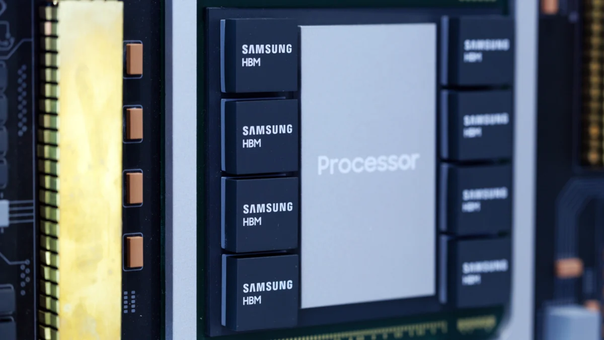
By allowing HBM4 to remain on a more traditional, refined microbump roadmap, JEDEC has provided manufacturers like SK Hynix, Micron, and Samsung with a "breathing room" to maximize their existing yields. Consequently, hybrid bonding in memory has been pushed back to the HBM4E and HBM5 generations, expected to debut toward the end of the decade. This ensures that the memory industry avoids a "double-jump" in complexity—trying to master both the transition to 16-high stacks and the transition to hybrid bonding simultaneously.
Supporting Data: The Density Divide
| Technology | Interconnect Density (Signals/mm²) | Status |
|---|---|---|
| Standard TSV (Face-to-Back) | ~1,500 | Mainstream |
| Microbump (Traditional) | ~2,000 – 4,000 | Mainstream |
| Hybrid Bonding (SoIC/Foveros) | ~14,000+ | High-Volume Logic |
The data confirms that the jump to hybrid bonding represents an order-of-magnitude shift. While logic designers are already utilizing this density to create "monolithic-like" 3D stacks, memory designers are balancing this potential against the sheer volume of memory throughput required for LLM training and real-time AI inference.
Official Responses and Industry Outlook
Industry analysts remain divided on whether the delay is a risk or a boon. Proponents of the current roadmap, including many within the JEDEC consortium, argue that the maturity of the microbump supply chain is sufficient to handle the bandwidth needs of HBM4.
"We are not choosing between performance and cost; we are choosing the right time for the right transition," noted a lead process engineer at a top-tier foundry. "If we forced hybrid bonding into HBM4, the cost of AI hardware would skyrocket before the ecosystem is ready to support the infrastructure."
Conversely, chip architects at companies like NVIDIA and AMD are closely watching the scaling of TSMC’s SoIC. As logic chips continue to demand faster access to data, the physical "wall" created by microbumps will eventually become the primary bottleneck for AI performance. The consensus is that while HBM4 may bypass hybrid bonding, HBM5 will likely be unable to do so. The physics of memory bandwidth simply leaves no other path forward.
Implications: The Road to 2030
The implications of this industry split are profound:
- Cost Stabilization: By deferring hybrid bonding in memory, the semiconductor industry avoids a sudden spike in HBM production costs, keeping AI development affordable for a wider range of enterprise customers through 2027.
- Infrastructure Bifurcation: Foundries will continue to operate two distinct packaging pipelines. Logic-centric hybrid bonding will continue to shrink toward the 4.5-micron target by 2029, while memory packaging will remain focused on vertical scaling (stack height) until the shift to hybrid bonding becomes mandatory.
- The Rise of Specialized Ecosystems: Companies that invest early in hybrid bonding equipment and materials, such as specialized wafer polishing and bonding machinery manufacturers, will find themselves in a dominant position as the memory industry eventually migrates to the technology for HBM4E and HBM5.
Conclusion
The postponement of hybrid bonding in memory is a tactical retreat, not a strategic defeat. It allows the industry to focus its engineering resources on the immediate goal of stacking more layers of memory while logic manufacturers perfect the copper-to-copper interconnection process. As we look toward 2030, the convergence of these two paths—the ultra-dense logic stacks and the high-bandwidth memory stacks—will represent the true "holy grail" of 3D integration. Until then, the semiconductor industry continues its methodical march, balancing the desperate need for performance with the cold, hard realities of manufacturing economics.