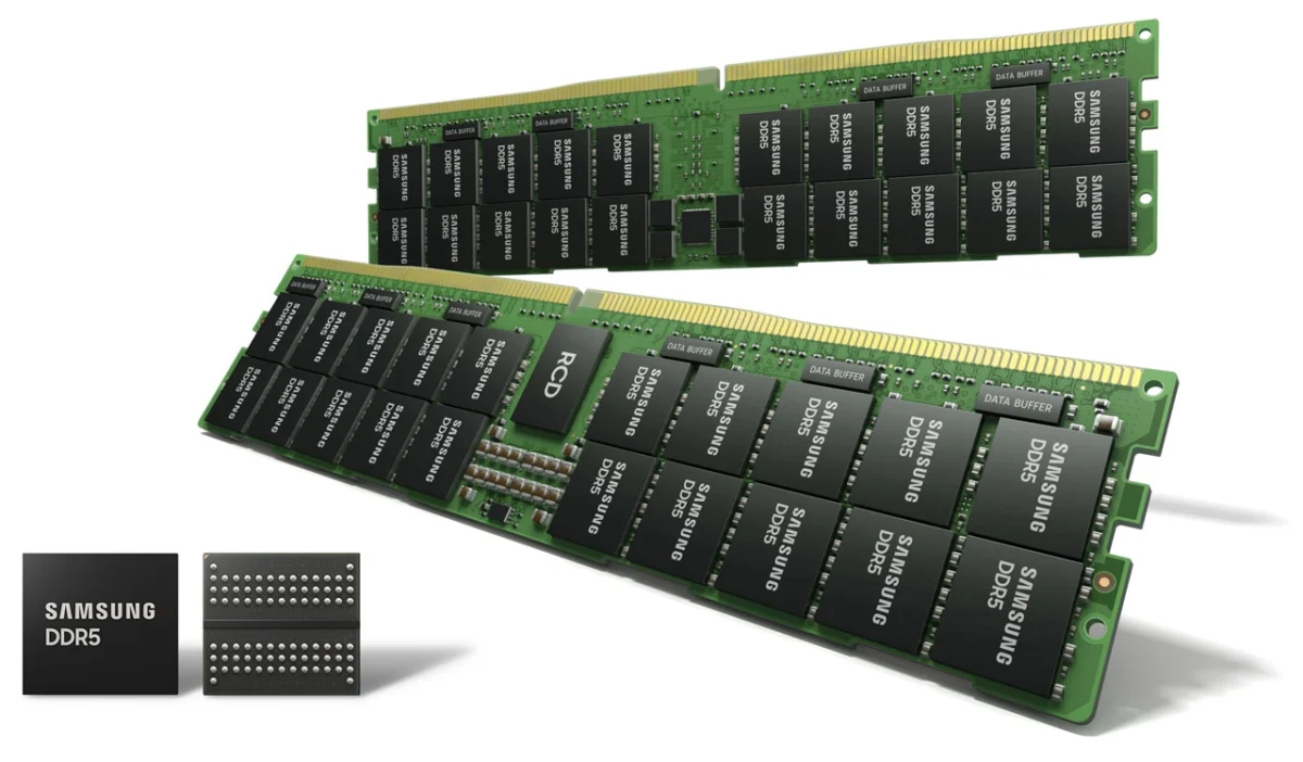
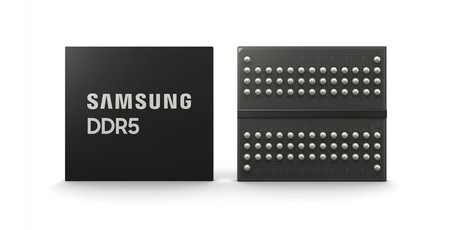
The semiconductor industry is currently navigating a period of unprecedented transformation. As the global demand for high-performance computing, artificial intelligence (AI), and massive data processing continues to skyrocket, the limitations of current memory technology have become a primary bottleneck. Today, Samsung Electronics has taken a definitive step toward breaking that barrier, announcing the start of mass production for its industry-leading 14-nanometer (nm) Extreme Ultraviolet (EUV) DDR5 DRAM.
This development marks a significant evolution in memory architecture, promising to deliver the highest density and fastest data transfer rates currently available on the market. As the industry transitions from the mature DDR4 standard to the more robust and efficient DDR5, Samsung’s latest technological leap positions the company at the vanguard of the next generation of computing infrastructure.
The Chronology of Innovation: From EUV Exploration to Mass Production
Samsung’s journey to the 14nm EUV process did not happen overnight. It is the result of years of rigorous research and development in photolithography and transistor scaling.
In 2020, Samsung made headlines by becoming the first company in the industry to successfully ship EUV-based DRAM. This milestone was the proving ground for the technology, confirming that EUV lithography could be applied to memory production to solve the scaling challenges that traditional Deep Ultraviolet (DUV) processes could no longer address as efficiently.
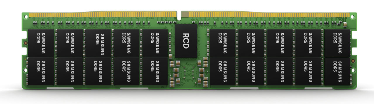
Following the success of that initial implementation, Samsung engineers pushed for further miniaturization. By refining their EUV application, the company has now successfully scaled its DRAM architecture down to 14nm. This transition is not merely a reduction in size; it represents a fundamental change in how memory cells are fabricated. By employing five distinct layers of EUV technology, Samsung has achieved the highest density of any DRAM currently in production, effectively condensing more computing power into a smaller physical footprint than ever before.
Supporting Data: By the Numbers
The technical specifications of the new 14nm EUV DDR5 DRAM are, by any metric, impressive. To understand the leap in performance, one must look at the comparative data between the outgoing DDR4 standard and the incoming DDR5 generation.
Performance Benchmarks
- Data Transfer Rates: The new DDR5 modules are capable of reaching speeds of up to 7.2 gigabits per second (Gbps). For context, standard DDR4 modules operate at roughly 3.2 Gbps. This effectively more than doubles the bandwidth, providing the "data pipes" necessary for high-bandwidth applications like 8K video editing and large-scale AI model training.
- Productivity and Efficiency: According to internal testing conducted by Samsung, the shift to 14nm EUV technology results in a 20 percent increase in overall productivity compared to the previous generation of DRAM. Perhaps even more importantly, the power efficiency of these modules has improved by a similar 20 percent. In a world where data centers are increasingly concerned with power consumption and thermal management, this increase in efficiency is as critical as the speed gains.
- Density Scaling: Samsung’s roadmap includes plans to refine this 14nm output to achieve an Integrated Circuit (IC) density of 24 gigabits (Gb). This evolution is expected to pave the way for massive 768GB DDR5 DIMMs, a capacity that was previously the domain of specialized, expensive server-grade hardware.
Official Responses and Strategic Vision
The significance of this launch was underscored by Jooyoung Lee, Senior Vice President and Head of the DRAM Product & Technology team at Samsung Electronics. In an official press statement, Lee emphasized that the achievement of extreme miniaturization via the 14nm EUV process is a "milestone" that addresses the specific needs of a "data-driven world."
"With the application of our 14nm EUV technology, we are not just making smaller memory; we are enabling the next generation of 5G, AI, and metaverse applications," Lee stated. The company’s messaging highlights a shift in strategy: moving away from purely incremental speed bumps toward a holistic focus on density and power efficiency, which are the primary limiting factors for modern hyperscale data centers and advanced workstations.
Samsung’s leadership believes that as the "metaverse" and AI-driven automation move from theoretical concepts to tangible, everyday infrastructure, the reliance on high-density, low-latency memory will become absolute. By establishing mass production now, Samsung aims to capture the lion’s share of the market as enterprise and consumer platforms migrate to DDR5-compatible chipsets.
Implications for the Market: The Cost of Progress
While the technical advancements are cause for celebration among technologists, the immediate impact on the consumer market comes with a caveat: the "early adopter tax."
The Motherboard Dilemma
As we move into the next generation of computing, such as the transition to Intel’s Alder Lake-S architecture, the industry is facing a temporary period of bifurcation. Motherboard manufacturers, including Asus, have been spotted registering dual-standard support. For example, the Asus Prime Z690-A, Z690-P, and Z690-V boards have been seen with ‘D4’ variants. This indicates that manufacturers are anticipating a slow transition, offering consumers the choice between existing, cheaper DDR4 memory and the high-performance, higher-cost DDR5 standard.
Pricing Realities
The cost of early adoption is currently quite steep. A recent listing on Newegg for a GeIL Polaris RGB SYNC 32GB (2 x 16GB) DDR5-4800 kit was priced at US$349.99. Similar pricing patterns have been observed in international markets, with listings in Japan reaching approximately 45,174 JPY. When converted to British Sterling, these prices hover between £250 and £300 for a 32GB kit.
This pricing significantly exceeds the cost of current-generation high-speed DDR4 memory, confirming that the initial rollout of DDR5 will be targeted at enthusiasts, power users, and enterprise clients who require the absolute cutting edge of performance. As mass production ramps up and the yields on 14nm EUV processes stabilize, analysts expect these prices to moderate, though a premium for DDR5 is likely to persist throughout the initial launch cycle.
Future Outlook: The Road Ahead
The transition to 14nm EUV DDR5 DRAM is more than just a specification update; it is a foundational shift for the digital economy. As Samsung scales its production, we are likely to see the following trends emerge over the next 18 to 24 months:
- Mainstream Capacity Expansion: While initial DIMMs are expected to be limited to 64GB, the eventual introduction of 24Gb ICs will normalize high-capacity memory configurations in mainstream consumer PCs.
- Server-Side Revolution: The 768GB DIMM potential will allow data centers to fit significantly more RAM into the same server rack space, reducing the physical footprint of massive cloud computing farms.
- Standardization of Speed: As 7.2Gbps becomes the new baseline, software developers will begin to optimize applications—particularly those in the AI and creative spaces—to utilize the expanded bandwidth, further driving the need for DDR5 upgrades.
In conclusion, Samsung’s mass production of 14nm EUV DDR5 DRAM is a clear signal that the industry is ready to move beyond the constraints of previous-generation memory. While the current market entry prices suggest that this technology is currently reserved for the enthusiast tier, the trajectory is clear: 14nm EUV is set to become the standard for the next generation of global computing. Whether it is powering the complex simulations of the metaverse or the real-time processing required by 5G networks, Samsung’s latest innovation provides the critical infrastructure upon which the future of technology will be built. As the supply chain matures and costs eventually decline, the broader impact of this 14nm leap will be felt by every user, from the casual consumer to the enterprise data architect.