 Lina Irawan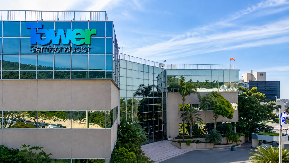
In a landmark move that underscores the shifting tides of global semiconductor manufacturing, Israeli foundry giant Tower Semiconductor has announced a massive $4 billion investment plan to transform its Japanese operations into a global nerve center for optical-connectivity chips. By partnering with the Japanese government, Tower aims to radically scale its output, positioning itself at the forefront of the burgeoning high-speed data transmission market. This ambitious "dual-track" strategy, aimed at achieving a 40-fold increase in production capacity by 2029, represents not only a significant capital injection but a fundamental shift in how the semiconductor industry prepares for the demands of the AI and data center era.
The Core Facts: A Strategic Reshaping
The centerpiece of this initiative is a collaborative investment between Tower Semiconductor and the Japanese government, totaling $4 billion. The primary objective is to convert and expand Tower’s regional fabrication facilities (fabs) into a specialized manufacturing powerhouse focused on silicon photonics and optical connectivity semiconductors.
Optical connectivity is the backbone of the next generation of data centers. As AI clusters and hyperscale computing environments require faster data throughput and lower energy consumption, traditional copper-based interconnects are reaching their physical limits. Silicon photonics—which uses light to transmit data across chips—is the industry’s answer to this bottleneck. Tower’s decision to dedicate its Japanese footprint to this technology is a calculated bet that the demand for high-speed optical transceivers will experience exponential growth over the next five years.
The expansion is categorized as a "dual-track" effort:
- Repurposing and Optimization: The company plans to bring an idled fab back online, retrofitting it for modern optical manufacturing requirements. Simultaneously, it will maximize the output of its existing 300mm wafer facility.
- Future-Proofing: Beyond the immediate upgrades, the roadmap includes the construction of an additional 300mm fab. By the end of 2029, these efforts are projected to boost Tower’s Japanese capacity to an impressive 45,000 300mm wafer-starts per month.
Chronology of the Investment
The roots of this expansion lie in the strengthening ties between Israeli tech firms and Japan’s aggressive semiconductor subsidy programs. Japan, seeking to reclaim its status as a dominant chip-manufacturing hub, has been actively courting global foundries to rebuild its domestic industrial base.
- Initial Engagement: Discussions between Tower and the Japanese government gained momentum throughout the last fiscal year, as Japan’s Ministry of Economy, Trade and Industry (METI) identified "optical semiconductors" as a critical strategic priority.
- The Restructuring Phase (2024): Tower began the internal process of restructuring its Japanese subsidiary operations, aligning local talent and infrastructure with the goal of high-volume photonics manufacturing.
- The $4 Billion Commitment: Following internal audits and government approval, the investment package was finalized. The influx of capital is expected to start hitting the regional fabs by the second half of 2024, with the first phase of capacity expansion beginning in early 2025.
- The 2029 Milestone: The project is phased over five years, with the final phase—bringing the new, state-of-the-art 300mm facility to full capacity—slated for completion by 2029.
Supporting Data: Why Optical Connectivity?
The semiconductor industry is currently undergoing a "photonic revolution." According to industry analysis, the market for silicon photonics is expected to grow at a Compound Annual Growth Rate (CAGR) of over 20% through 2030. Tower’s decision to commit to 45,000 wafers per month is a direct response to this data.
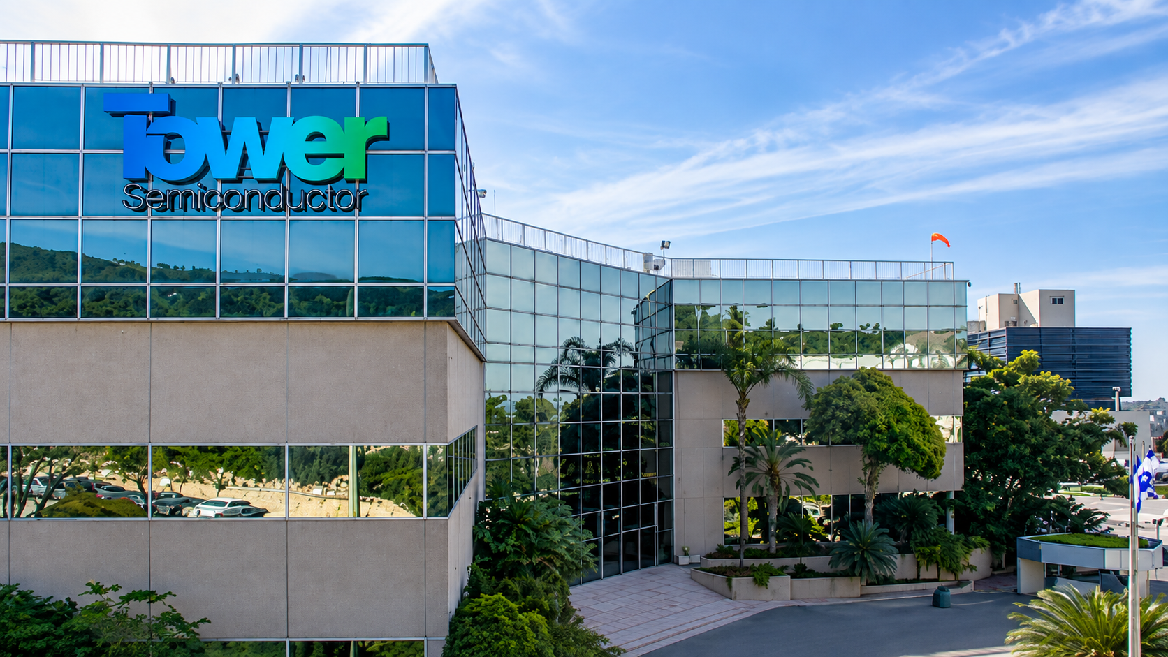
To understand the scale, one must look at the transition from 200mm to 300mm production. 300mm wafers offer significantly better economies of scale and are the industry standard for high-performance chips. By focusing on 300mm, Tower is ensuring that its Japanese hubs can compete with the world’s most advanced foundries.
Furthermore, the "40-fold increase" metric is the most striking statistic of the announcement. This figure accounts for both the increased throughput of the new facilities and the higher technical complexity of the chips being produced. By consolidating its optical manufacturing in Japan, Tower is creating a "hub-and-spoke" model where the intellectual property, design kits, and manufacturing capabilities are localized, significantly reducing the "time-to-market" for their global clientele.
Official Responses and Stakeholder Sentiment
The partnership has been met with optimism from both the Japanese government and the broader semiconductor ecosystem.
A spokesperson for the Japanese Ministry of Economy, Trade and Industry noted that the collaboration aligns with Japan’s "Semiconductor and Digital Industry Strategy," which seeks to secure a stable supply chain for advanced components. "By welcoming Tower’s expansion, we are not just adding manufacturing capacity; we are adding a critical layer of technical capability in photonics that will make Japan an indispensable partner in the global AI infrastructure," the spokesperson stated.
From Tower Semiconductor’s perspective, the move is a vital evolution. "The demand for high-speed, low-power data transmission is insatiable," noted an executive source within the company. "By investing in Japan, we are leveraging a highly skilled workforce, established industrial infrastructure, and strong government support to meet the needs of the next decade of data center growth."
Implications for the Global Semiconductor Landscape
The implications of this $4 billion investment extend far beyond the borders of Japan and the balance sheet of Tower Semiconductor.
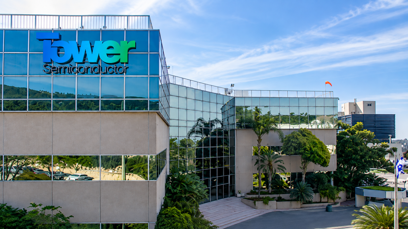
1. Diversification of the Supply Chain
The semiconductor industry has spent the last several years attempting to de-risk its supply chains, which were previously over-concentrated in a few geographic regions. By building a massive optical hub in Japan, Tower is providing a high-capacity alternative for companies looking to source critical chips outside of the traditional Taiwan-centric manufacturing model.
2. A Shift Toward Specialized Foundries
Tower Semiconductor has long been recognized as a leader in "analog" and specialty process technologies. This move signals a broader trend: as Moore’s Law becomes more difficult to scale in digital logic (CPUs/GPUs), the value of specialty chips—such as those for optical connectivity, power management, and RF (radio frequency)—is skyrocketing. Tower is effectively cornering a niche that is becoming increasingly "mainstream" due to the AI boom.
3. Economic Impact on Japan
For Japan, this investment is a major win. The facility expansion is expected to create thousands of high-tech jobs and foster a local ecosystem of component suppliers, testing facilities, and research institutions. It validates the "Japan 2.0" strategy of creating a self-sustaining semiconductor cluster that can attract both foreign capital and top-tier engineering talent.
4. The "AI Bottleneck"
Perhaps the most significant implication is the technological one. If the industry fails to solve the energy and heat dissipation problems associated with traditional data transmission, the progress of AI and Large Language Models (LLMs) will stall. By providing the manufacturing capacity to mass-produce optical connectivity chips, Tower is positioning itself as a silent enabler of the AI revolution.
Conclusion
Tower Semiconductor’s $4 billion investment in Japan is more than a mere expansion; it is a strategic alignment with the future of global infrastructure. By betting heavily on optical connectivity and 300mm wafer technology, the company is positioning itself to be a linchpin in the data-driven world of the 2030s. As the facilities in Japan come online over the next five years, the global tech industry will be watching closely to see if this massive bet on photonics delivers the performance gains required to power the next generation of artificial intelligence.


 Laily UPN
 Layla Zulfa