In a significant move aimed at fortifying its competitive position in the global semiconductor market, Intel has announced a major leadership restructuring within its Foundry division. The company is splitting its foundry operations into two distinct domains: "Front-End" and "Back-End." To lead the latter, Intel has tapped industry heavyweight Seok-Hee Lee, marking a high-profile return for an executive who spent a decade at Intel before rising to the top echelons of the South Korean semiconductor industry.
This structural shift signals a pivot in Intel’s strategy, acknowledging that the complexity of modern chip manufacturing requires a more specialized, bifurcated approach. As the company pushes toward its ambitious "Intel 14A" process node, the separation of wafer fabrication from advanced packaging suggests that Intel is preparing to be more aggressive in selling its services to external clients—a move essential to its long-term survival as a foundry provider.
The Leadership Split: A Strategic Bifurcation
Under the new organizational framework, Intel Foundry will be led by two distinct Executive Vice Presidents. Naga Chandrasekaran, who previously held the reins of the entire foundry unit, will now focus exclusively on "Front-End" operations. This encompasses the critical, highly complex world of wafer fabrication—the lithography, deposition, and etching processes required to create the transistors themselves. With the industry’s eyes currently fixed on the development of Intel 18A and the upcoming 18A-P, as well as the transition toward the 14A node, Chandrasekaran’s focus remains on the "bleeding edge" of logic manufacturing.
Seok-Hee Lee, meanwhile, will lead the "Back-End" operations, specifically taking charge of Advanced Packaging. This division is tasked with the integration of chiplets, the use of proprietary technologies like EMIB (Embedded Multi-die Interconnect Bridge) and Foveros, and the final assembly of heterogeneous compute architectures. By elevating Advanced Packaging to an equivalent leadership tier, Intel is signaling that its ability to stack and interconnect silicon is just as vital as the process nodes used to create it.
Chronology: The Evolution of Intel Foundry
The journey to this organizational shift has been marked by rapid personnel changes and a desperate need for operational efficiency.
- The Early Years (2000s–2010s): Seok-Hee Lee originally spent ten years at Intel during a period when the company was arguably at the peak of its global dominance. His departure marked a significant loss of internal expertise at the time.
- The Rise at SK Hynix and SK On: After leaving Intel, Lee played a pivotal role in the South Korean semiconductor surge. He eventually climbed the ranks to become CEO of SK Hynix, where he managed large-scale memory production and R&D. Most recently, he served as the President and CEO of SK On, the battery manufacturing subsidiary of the SK Group.
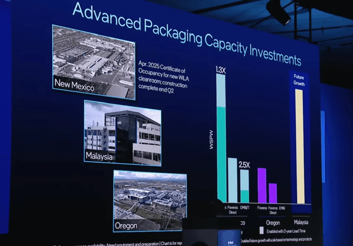
- The Foundry Pivot (2021–2024): Intel CEO Pat Gelsinger launched IDM 2.0, aiming to open the company’s doors to external customers. The company invested heavily in manufacturing sites globally, including the massive expansion in Malaysia, specifically tailored for back-end assembly and test operations.
- Present Day (2024/2025): The decision to bring Lee back underscores a realization that the "foundry" business is not just one job—it is two. The split is intended to ensure that manufacturing excellence does not bottleneck packaging innovation, and vice-versa.
Supporting Data: Why Packaging Matters
Intel’s focus on Advanced Packaging is not merely a technical choice; it is an economic necessity. In the era of AI and High-Performance Computing (HPC), it is becoming increasingly difficult to build a single, massive "monolithic" chip that remains cost-effective and high-yielding. Instead, companies like NVIDIA, AMD, and Apple are increasingly turning to chiplet architectures, where different parts of a processor (CPU, GPU, I/O, Cache) are manufactured on different nodes and then "packaged" together.
Intel’s investment in the "Pelican" project—a massive packaging complex in Malaysia that recently went online—is a direct hedge against the industry’s reliance on TSMC. By offering a comprehensive suite of packaging services, Intel hopes to attract clients who may not yet be ready to use Intel’s wafer fabs but are eager to utilize its world-class packaging technologies.
Industry analysts point out that Intel has a competitive edge here. Through technologies like EMIB and Foveros, Intel has a years-long head start in the "chiplet" ecosystem. If the company can successfully commoditize these services, it could capture a significant portion of the AI accelerator market, even if those accelerators are built using non-Intel silicon.
Official Responses and Internal Sentiment
While Intel has not issued a detailed public manifesto regarding this split, the move is widely seen by market observers as a necessary concession to the realities of high-stakes manufacturing. Insiders suggest that by separating the roles, Intel is attempting to replicate the specialization found in successful "pure-play" foundry competitors, while still retaining the benefits of an integrated device manufacturer.

"We are aligning our leadership structure to the specialized needs of modern silicon," a representative indicated in recent briefings. The focus on "Front-End" and "Back-End" is meant to provide clearer KPIs (Key Performance Indicators) for leadership. Chandrasekaran’s focus remains fixed on the "process-per-watt" efficiency of the 18A-P and 14A nodes, while Lee is tasked with ensuring that Intel’s packaging capacity can scale rapidly to meet the demand from hyperscalers like Google, Microsoft, and Amazon.
Implications: A New Era for Intel?
The implications of this structural change are profound.
1. The Battle for External Customers
Intel’s greatest hurdle remains convincing external competitors to entrust their designs to a direct rival. By creating a more distinct Foundry division with specialized leadership, Intel is attempting to present a more professional, "neutral" facade. If a client like Apple or Nvidia chooses Intel for packaging, they need to know that the packaging team is operating with the same level of confidentiality and autonomy as a dedicated, independent OSAT (Outsourced Semiconductor Assembly and Test) provider.
2. The 14A Node as a Make-or-Break Moment
The success of Naga Chandrasekaran in the Front-End division will be measured primarily by the yield and performance of the Intel 14A node. If Intel can demonstrate a competitive manufacturing process that rivals TSMC’s N2 or A16 nodes, it could fundamentally change the trajectory of the company. However, if the development hits delays, the pressure on the leadership team will intensify.
3. The "Packaging-First" Strategy
There is a growing school of thought that Intel might be more successful in the short term as a packaging provider than as a wafer manufacturer. Given the high demand for AI chips, if Intel can establish its packaging facilities as the "industry standard" for high-bandwidth memory (HBM) and processor integration, it could become a vital cog in the global AI hardware machine, regardless of where the actual transistor logic is etched.
4. Leadership Stability
The return of Seok-Hee Lee is a morale booster for the engineering teams. It signals that Intel is willing to reach back into its history to find talent that understands both the company’s internal culture and the rigorous demands of the global semiconductor market. However, it also highlights the internal tension: when a company feels the need to reach out to former executives to help steer the ship, it confirms that the current crisis is one that requires deep, historical expertise to solve.
Conclusion: A Bifurcated Path Forward
Intel’s split of its foundry leadership represents the most significant organizational change in the company’s recent history. By acknowledging that wafer fabrication and advanced packaging are two distinct, equally critical pillars of modern computing, Intel is attempting to streamline its path toward the Intel 14A node and beyond.
The success of this strategy will depend on the synergy between Chandrasekaran and Lee. If they can manage the "Front-End" for speed and efficiency while scaling the "Back-End" for versatility and volume, Intel may finally be able to shed its reputation as a struggling legacy giant and reclaim its status as the backbone of the global semiconductor industry. For now, the eyes of Wall Street and the tech world remain fixed on these two leaders, waiting to see if this dual-engine approach can provide the necessary thrust to pull Intel out of its current slump.