
At the 2026 Hot Chips conference, Intel unveiled its latest strategy to reclaim the entry-level computing market with the "Wildcat Lake" architecture. While budget-tier processors are historically characterized by "N-1" designs—recycling older, lower-cost silicon—Intel has taken a bold, counter-intuitive approach. By deploying its most advanced compute node for a budget product, Intel has fundamentally shifted how it approaches cost-efficiency, utilizing the Universal Chiplet Interconnect Express (UCIe) to turn a potential fiscal liability into an industry-leading innovation.
The Genesis of a New Budget Strategy
Historically, the "budget" designation in the processor world was synonymous with compromise. Manufacturers would take legacy architecture, disable portions of the cache or core count to improve yields, and rebrand it for lower-cost systems. Intel’s Wildcat Lake departs from this stagnant methodology. During his opening keynote at Hot Chips 2026, Lance Hacking, the lead engineer behind the project, revealed that the company faced a critical crossroads: pursue a traditional, monolithic budget design or embrace the risks of a Multi-Chip Package (MCP).
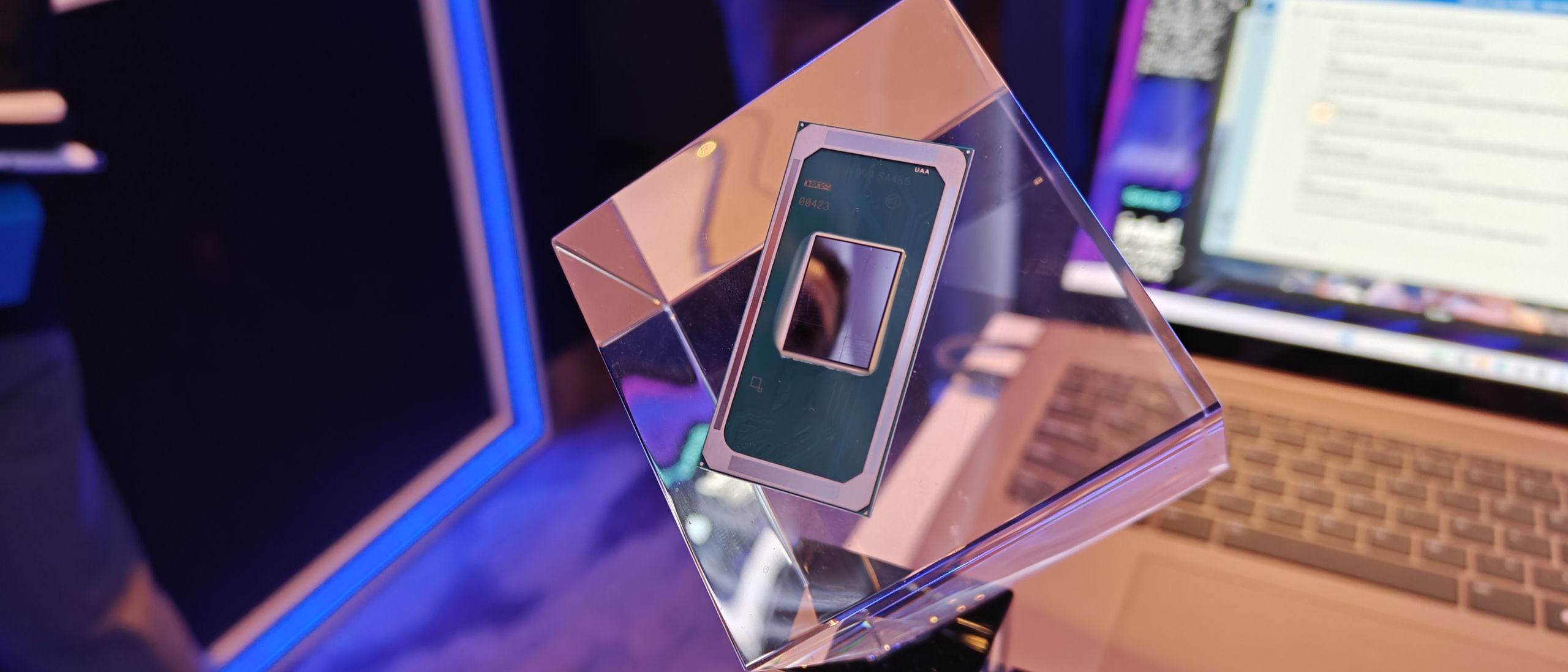
Intel opted for the latter, but with a specific, forward-thinking twist. While Intel’s sophisticated Foveros 3D packaging technology is reserved for high-end server and enthusiast-grade silicon, it was deemed too expensive for a price-sensitive entry-level chip. Instead, Intel turned to the UCIe specification—an open-standard interconnect protocol that debuted in 2022. By integrating UCIe, Intel not only made Wildcat Lake viable from a cost perspective but also established a blueprint for how future chiplet-based processors could be manufactured without the overhead of proprietary, locked-in communication standards.
Chronology of Development: From Concept to Silicon
The planning for Wildcat Lake began in early 2022, shortly after the initial industry push for an open-standard chiplet interconnect. The development cycle can be categorized into three distinct phases:
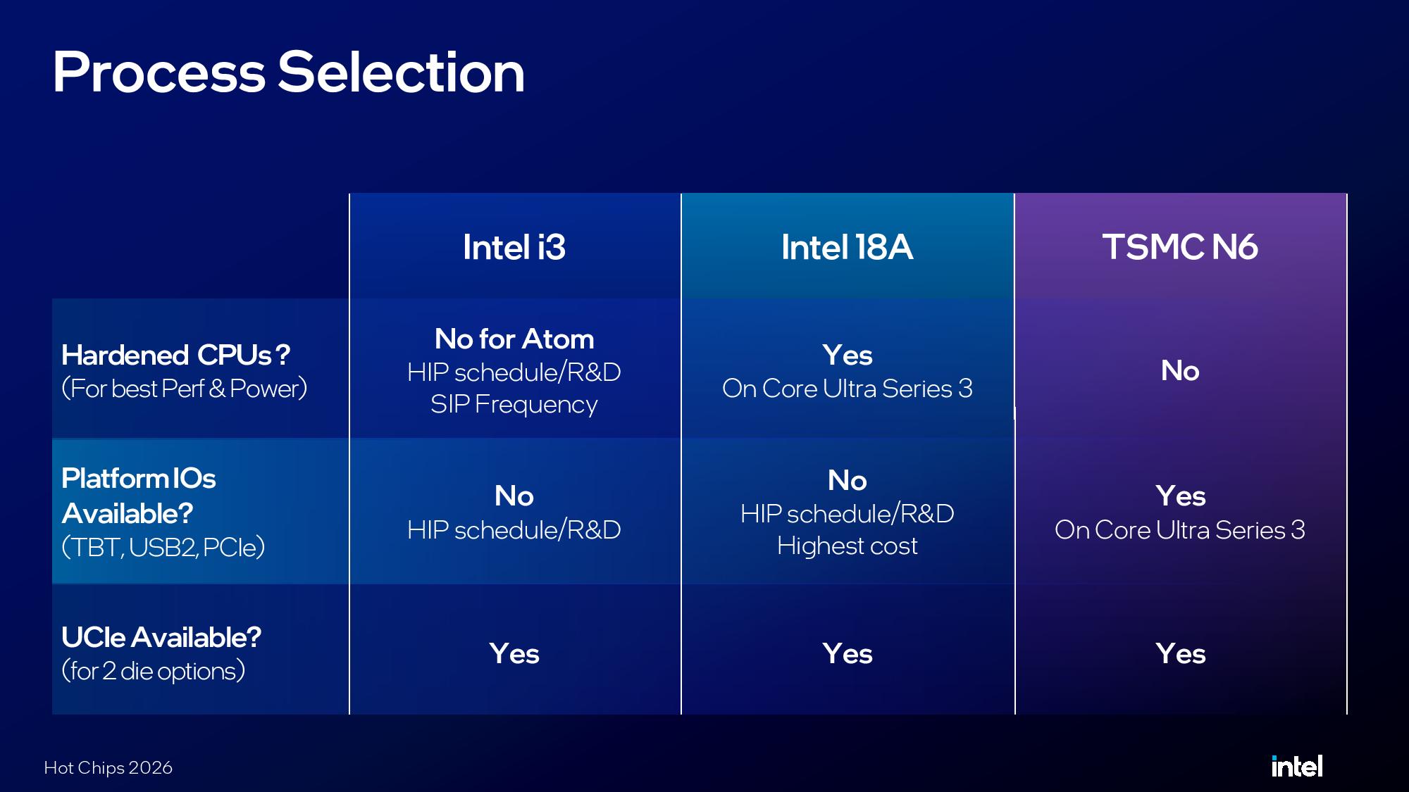
- Architecture Selection (2022–2023): Intel engineers focused on the feasibility of integrating 18A compute dies with N6 (Node 6) I/O dies. This period was defined by the decision to move away from monolithic architectures, which were becoming increasingly expensive to produce as node sizes shrank.
- UCIe Optimization (2024): The engineering team spent the bulk of 2024 refining the UCIe implementation. This was the most challenging phase, as the team had to compensate for the higher power requirements and increased die area associated with the UCIe interface compared to traditional, tightly coupled monolithic buses.
- Refinement and Yield Management (2025–2026): In the final year before launch, Intel focused on "binning" and bill-of-materials (BOM) reduction. By stripping away non-essential features (such as dedicated camera PHYs and auxiliary controllers), Intel successfully hit the aggressive price targets required for the budget laptop segment.
The Technical Backbone: UCIe and Die-Level Optimization
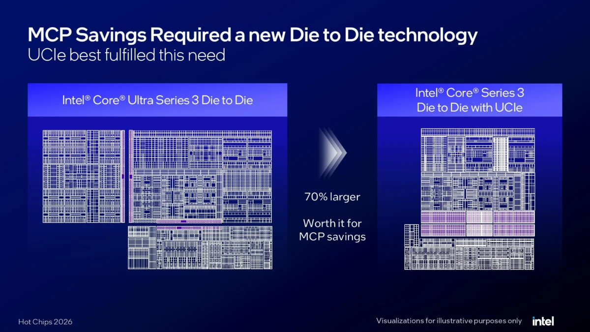
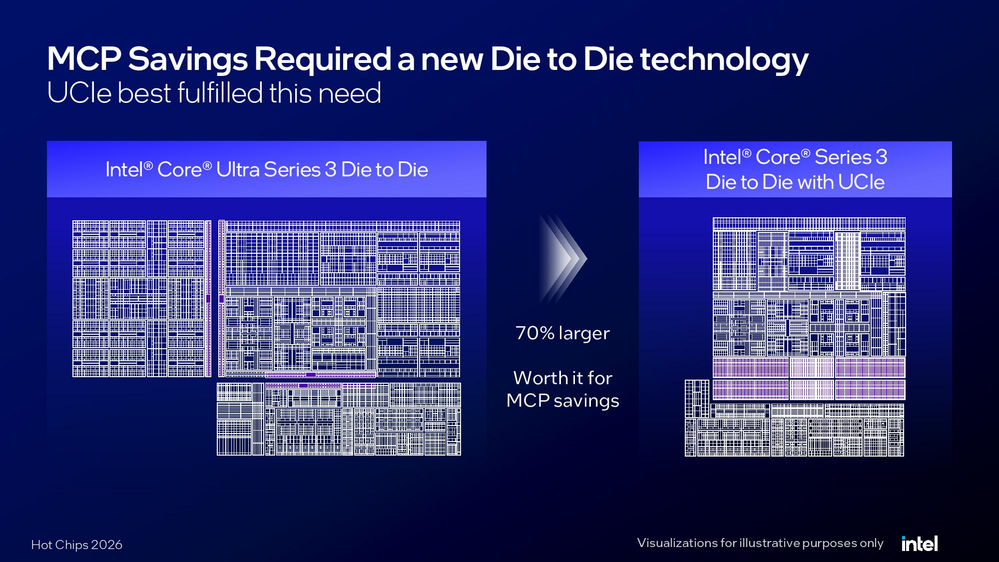
The integration of UCIe was not merely a cost-saving measure; it was a necessary architectural pivot. Because Wildcat Lake lacks a base die for interconnect communication, the interface occupies a significantly larger footprint than the one seen in Intel’s more premium "Panther Lake" processors. Intel reports that the interconnect in Wildcat Lake is roughly 70% larger than its predecessor’s, a deliberate trade-off made to ensure long-term manufacturing flexibility.
Power Management and the Display Engine
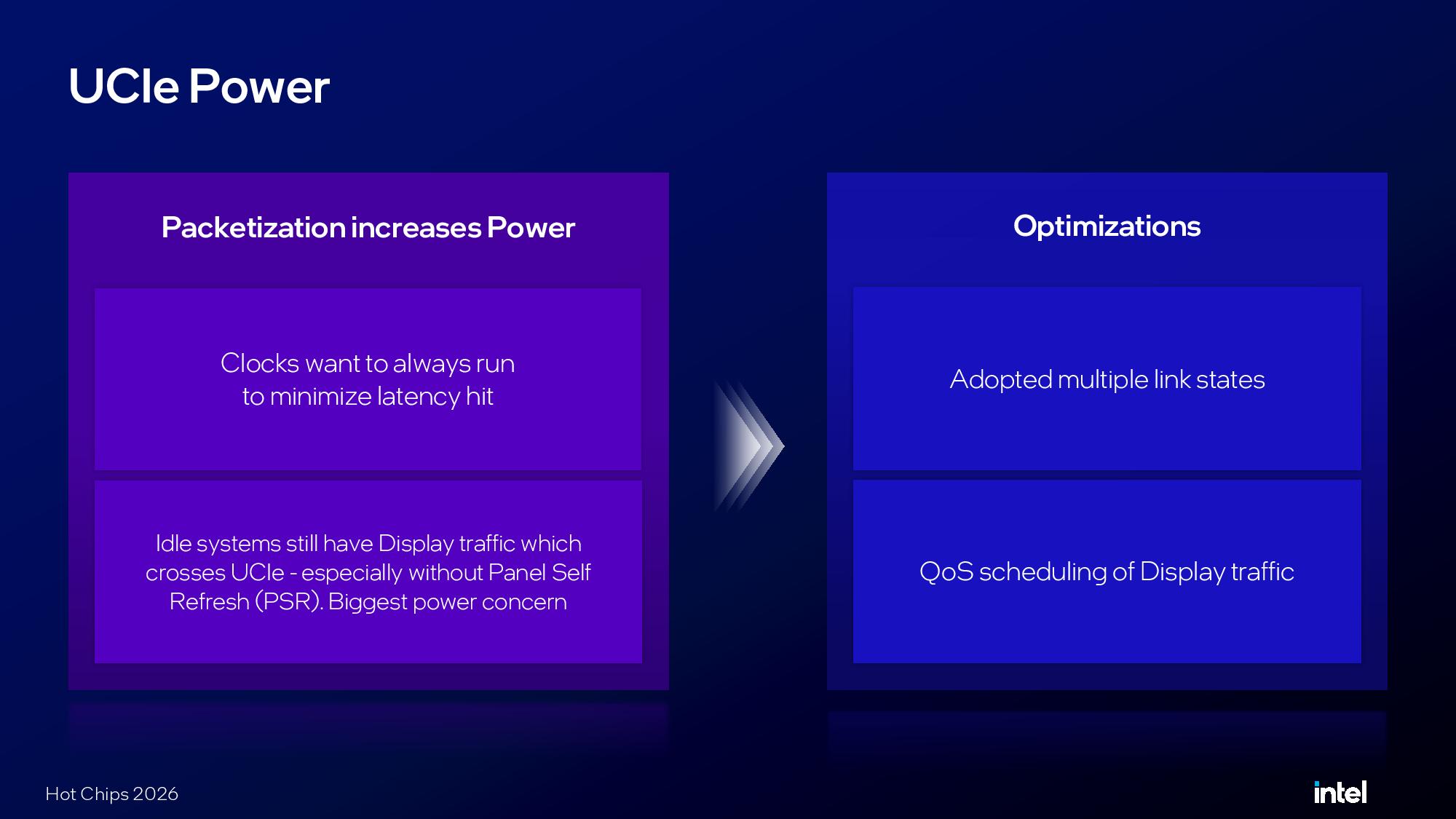
One of the primary concerns regarding UCIe in mobile devices is power efficiency. Because UCIe is packetized, high-frequency data transmission across the chiplet boundary can quickly deplete a laptop’s battery. To mitigate this, Intel developed a specialized buffer system.
The system addresses the "idle power" problem by placing a buffer before the UCIe link. This allows the display engine to hold panel refresh signals during idle states, preventing the need to keep the UCIe link active for static images. By adding this buffer alongside the traditional memory controller-to-display engine connection, Intel managed to maintain competitive battery life in a package that would otherwise have been power-prohibitive.
Strategic Die Trimming
To make space for the UCIe interface, Intel aggressively pruned the compute and I/O dies:
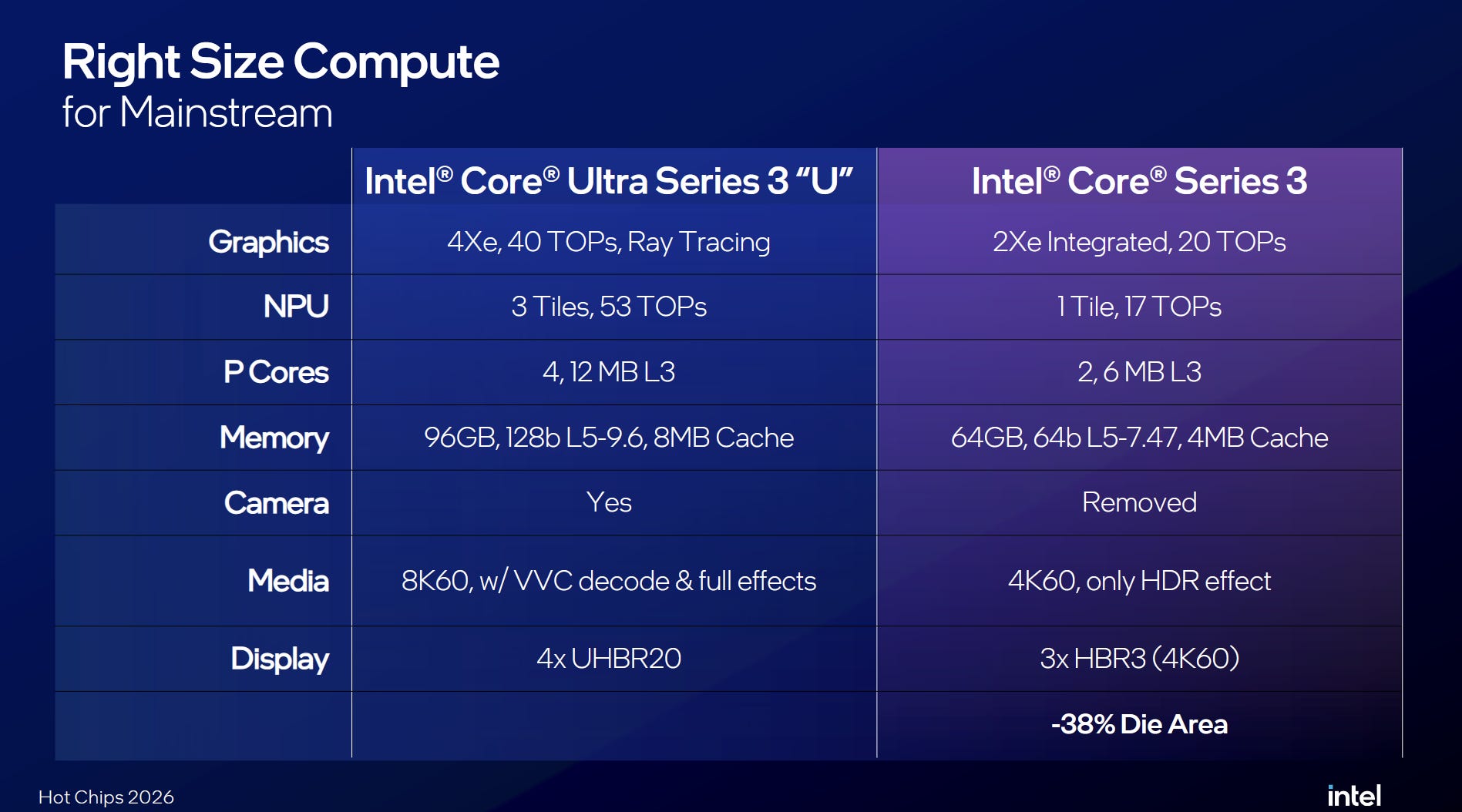
- Compute Die: The number of Xe cores was halved from four to two. The NPU (Neural Processing Unit) was reduced to a single tile, and ray-tracing accelerators were removed entirely. The memory controller was downgraded to a 64-bit bus, sacrificing some bandwidth for significantly lower power consumption and heat output.
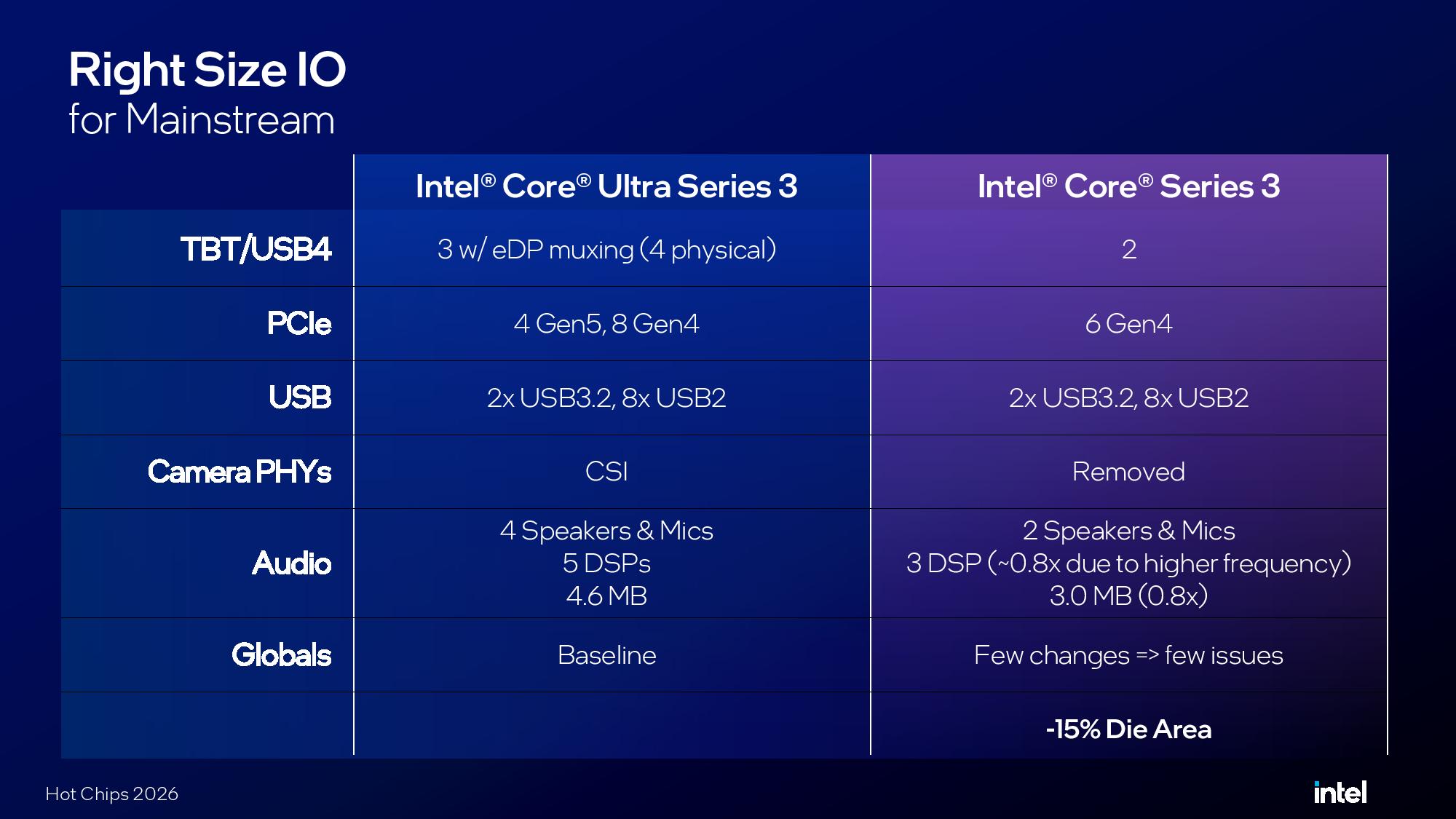
- I/O Die: By removing the camera PHY and reducing the number of available PCIe and USB lanes, Intel reclaimed 15% of the total I/O die area. The company placed the burden of camera integration on original equipment manufacturers (OEMs), further lowering the base silicon cost.
Official Stance: Intel’s Economic Philosophy
Intel’s presentation at Hot Chips 2026 highlighted that Wildcat Lake is a direct response to the "N-1" design fatigue. "We wanted to create a product that customers actually want," Hacking noted, "not just a product that fills a hole in our SKU list."
Intel’s strategy for cost recovery was highly disciplined. Rather than attempting to "save" every defective chip through aggressive binning, Intel only performed recovery where it made economic sense. For example, a chip with a single working Performance-core (P-core) would be salvaged for the Core 3 304 model. However, Intel refused to compromise the LPE (Low-Power Efficiency) clusters or the I/O interface, as these components are central to the "low-power island" functionality that differentiates Wildcat Lake from competitors.
Market Implications and Competitive Landscape
The launch of Wildcat Lake positions Intel in a direct confrontation with Apple’s MacBook Neo and the rising tide of Qualcomm-based Windows machines. Both competitors utilize mobile-derived SoCs, which are generally efficient but lack the modularity that UCIe provides.
The "Project Firefly" Initiative
Expanding upon the Wildcat Lake design, Intel introduced "Project Firefly." This initiative aims to leverage the mobile supply chain to standardize budget laptop manufacturing. By integrating Wi-Fi 7 and USB PD (Power Delivery) controllers directly into the silicon, Intel has reduced the total bill of materials for its OEM partners. Furthermore, by opting for a 6-layer PCB design—down from the standard 8-layer boards—Intel has enabled manufacturers to produce thinner, cheaper, yet sufficiently capable laptops.
Innovation Amidst Turmoil
The success of Wildcat Lake is underscored by the 2026 Tom’s Hardware Innovation Award. In an industry currently navigating significant supply chain volatility and a shift toward ARM-based architectures, Intel’s commitment to an open, scalable standard like UCIe demonstrates a rare degree of foresight.
By refusing to settle for legacy silicon and instead embracing a modular, chiplet-based future for the entry-level market, Intel has effectively raised the bar for what a "budget" computer should be. Whether competitors will pivot to follow this model or continue to rely on the traditional N-1 approach remains to be seen, but the success of Wildcat Lake suggests that the chiplet revolution is no longer a luxury reserved for the high-end server room—it is now a fundamental requirement for the modern consumer PC.
Future Outlook
As we look beyond 2026, the implications of the Wildcat Lake architecture are profound. The ability to mix and match compute and I/O dies using a standardized interconnect like UCIe will likely allow Intel to iterate on its product stack much faster than in the past. If the company can successfully lower the cost of its 18A nodes through this modularity, it may find itself in a dominant position once again, forcing a broader industry shift toward universal, open-standard chiplet communication. For now, Wildcat Lake stands as a testament to the idea that innovation is most powerful when it is applied to the most mundane of tasks: making affordable, efficient, and reliable technology for the everyday user.