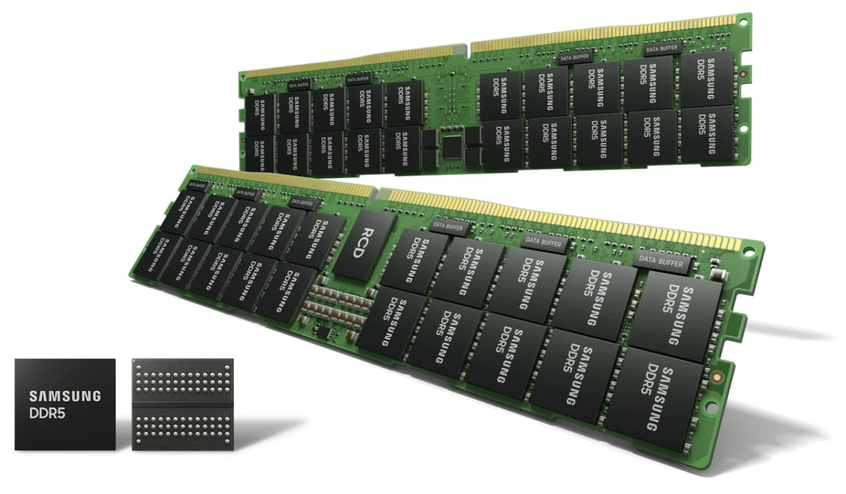
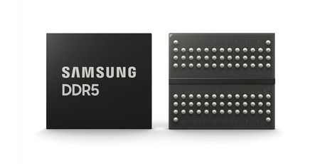
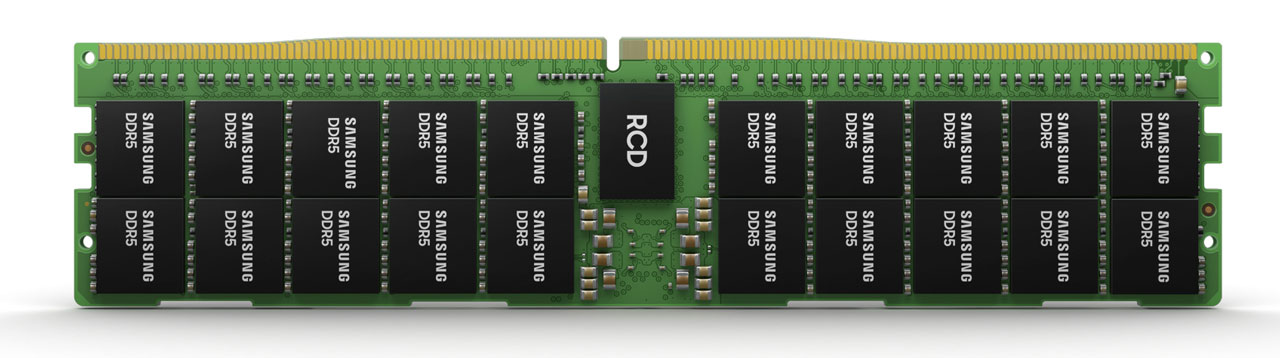
In a landmark development for the semiconductor industry, Samsung Electronics has officially commenced mass production of its most advanced memory solution to date: 14nm Extreme Ultraviolet (EUV) DDR5 DRAM. This milestone not only cements Samsung’s leadership in the global memory market but also signals a seismic shift in how computing hardware will handle the escalating demands of artificial intelligence, high-performance computing (HPC), and the burgeoning "metaverse." By successfully shrinking the process node to 14nm and incorporating a five-layer EUV architecture, Samsung has created the densest and most efficient DRAM currently available on the commercial market.
The Technological Leap: EUV and the 14nm Milestone
The transition to Extreme Ultraviolet (EUV) lithography represents one of the most significant hurdles in modern silicon manufacturing. While conventional deep ultraviolet (DUV) lithography has served the industry for decades, the physical limits of wavelength light necessitated a move to the shorter, more precise wavelengths of EUV to continue the march of Moore’s Law.
Samsung’s journey began in 2020, when it became the first manufacturer to ship EUV-based DRAM. Today, that foundation has evolved into a highly refined 14nm process. The integration of five distinct layers of EUV light application allows Samsung to achieve unprecedented levels of circuit complexity. By moving to this advanced node, Samsung is effectively increasing the density of the memory cells, which translates directly to higher performance, reduced power consumption, and greater scalability for future data-center and consumer applications.
A Chronology of Innovation: From DUV to 14nm EUV
To understand the magnitude of this achievement, one must look at the timeline of memory evolution:
- Pre-2020: The industry relied almost exclusively on DUV lithography. As nodes shrank toward the 10nm-class barrier, DUV required increasingly complex multi-patterning techniques, which introduced yield issues and physical limitations.
- 2020: Samsung officially broke the barrier by introducing EUV to the DRAM production process. This initial deployment served as a proof-of-concept for the viability of EUV at scale in memory manufacturing.
- 2021 (Current Milestone): Samsung pushes the envelope further by introducing the 14nm process node, specifically optimized for DDR5. This move is timed to coincide with the next generation of CPU architectures, such as Intel’s Alder Lake, which requires the bandwidth that only DDR5 can provide.
- Future Outlook: Samsung has already signaled its intent to further refine its 14nm output, with plans to increase integrated circuit (IC) density to 24Gb, potentially enabling massive 768GB DDR5 DIMM modules for enterprise-grade hardware.
Supporting Data: By the Numbers
The performance metrics associated with Samsung’s new 14nm DDR5 modules are stark when compared to the outgoing DDR4 standard. According to the company’s internal validation testing, the new memory offers significant improvements across several key performance indicators:
1. Throughput and Speed
The DDR5 standard is designed to deliver speeds that were previously considered impossible for consumer-grade memory. Samsung’s new modules are capable of reaching data transfer rates of up to 7.2 gigabits per second (Gbps). For perspective, the standard DDR4 modules that have powered the last half-decade of computing typically operate at roughly 3.2 Gbps. This represents more than a doubling of raw bandwidth, providing the "headroom" required for heavy data-processing tasks.
2. Efficiency and Productivity
Beyond raw speed, the 14nm EUV process offers a 20 percent improvement in overall productivity compared to previous-generation DRAM. Similarly, energy efficiency—a critical metric for data centers—has seen a corresponding 20 percent improvement. In an era where carbon footprints and power consumption are increasingly scrutinized, these marginal gains aggregate into massive savings for hyperscale cloud providers.
3. Density and Capacity
Samsung’s roadmap includes a push toward 24Gb density, which would allow for single-stick capacities far exceeding what is currently standard. While initial mainstream DDR5 DIMMs will likely top out at 64GB per stick, the long-term goal is to reach 768GB configurations, a leap that will redefine workstation capabilities.
Official Responses and Strategic Vision
Jooyoung Lee, Senior Vice President and Head of the DRAM Product & Technology team at Samsung Electronics, framed the announcement as a critical inflection point for the digital age. In an official press statement, Lee emphasized that this achievement is not merely about shrinking circuits; it is about enabling the next generation of computing.
"We have set an important milestone with our extreme miniaturization of DRAM," Lee stated. "Our 14nm EUV technology is the catalyst that will allow us to meet the surging demand in our data-driven world, specifically for 5G, AI, and the metaverse."
Samsung’s strategy is clear: by positioning itself as the primary supplier of the highest-density, fastest DDR5 modules, the company ensures its dominance in the enterprise, server, and premium consumer markets simultaneously.
Implications for the Consumer Market
While the technical specs paint a picture of a revolutionary upgrade, the real-world implications for the average consumer are nuanced, primarily due to the "early adopter tax."
The Cost of Innovation
As with any major transition in the PC industry, the move to DDR5 comes with a price premium. Early listings from retailers such as Newegg suggest that consumers should be prepared to pay a significant amount for the privilege of early adoption. A 32GB (2 x 16GB) kit of GeIL Polaris RGB SYNC DDR5-4800 was recently spotted listed at approximately US$349.99. In international markets, the pricing has shown similar trends, with Japanese retailers listing kits at prices that convert to between £250 and £300.
The Motherboard "Bridge"
Recognizing that the high cost of DDR5 may deter some users, motherboard manufacturers are taking a pragmatic approach. Companies like Asus are preparing to launch "bridge" platforms for the upcoming Intel Z690 chipsets. These boards are expected to arrive in two distinct variants: one offering native DDR5 support and another specifically designed to maintain compatibility with existing DDR4 memory.
This bifurcation of the market allows enthusiasts to upgrade to the latest CPU architectures—such as the Alder Lake-S series—without being forced into the prohibitively expensive DDR5 ecosystem immediately. It is a strategic hedge that acknowledges the current supply chain constraints and the high manufacturing costs associated with the new memory standard.
Conclusion: A New Foundation for the Digital Future
Samsung’s mass production of 14nm EUV DDR5 DRAM is more than just a specification bump; it is a foundational change in the architecture of modern computing. As we transition into a world defined by the massive data throughput requirements of AI and the metaverse, the bottleneck of memory bandwidth has become the industry’s primary concern.
By delivering a product that is faster, more efficient, and significantly denser than anything that came before, Samsung has successfully cleared the path for the next generation of hardware. While the high initial costs and the transitional nature of early motherboard support suggest that widespread adoption will take time, the trajectory is clear. The era of 14nm EUV is here, and it is set to define the performance benchmarks for the remainder of the decade. As these modules reach the hands of gamers, developers, and data scientists, the true potential of this silicon-based innovation will begin to manifest in every pixel of the metaverse and every calculation performed by artificial intelligence.