
The semiconductor industry is currently navigating one of its most consequential transition periods in history. As Moore’s Law encounters the physical limits of traditional manufacturing, the quest for ever-smaller, more energy-efficient, and more powerful transistors has pushed engineers to adopt increasingly exotic technologies. At the heart of this revolution lies Extreme Ultraviolet (EUV) lithography. After years of deliberate silence and strategic caution, TSMC—the world’s largest contract chipmaker—has officially confirmed its roadmap for the adoption of High-Numerical Aperture (High-NA) EUV lithography, signaling a major shift in its manufacturing strategy set for 2030.
The Strategic Shift: From Caution to Commitment
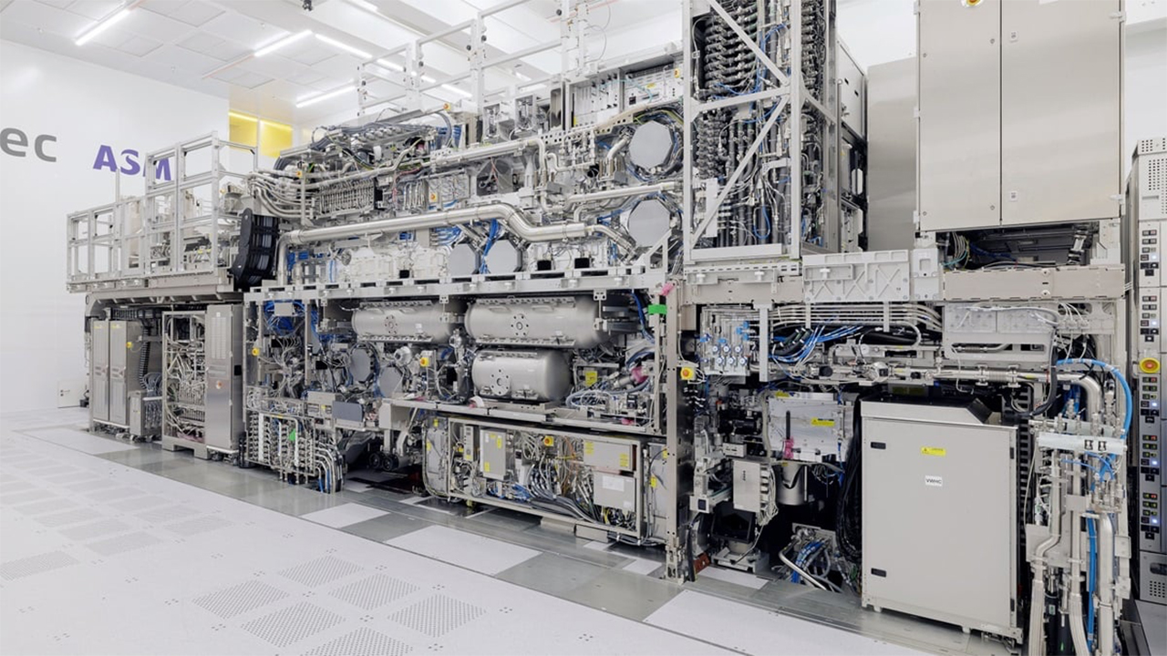
For nearly a decade, TSMC maintained a pragmatic, if not skeptical, stance regarding the immediate necessity of High-NA EUV tools. These machines, which feature a 0.55 numerical aperture compared to the 0.33 NA of current systems, are technological marvels priced at approximately $400 million per unit. While competitors like Intel leaned heavily into early adoption, TSMC’s engineering teams focused on optimizing existing Low-NA EUV infrastructure through innovative patterning and process refinement.
However, the laws of physics are unforgiving. As transistor architectures evolve toward increasingly complex Gate-All-Around (GAA) designs and, eventually, Complementary Field-Effect Transistors (CFETs), the resolution limits of standard 0.33 NA systems have begun to show their constraints. By announcing that it will integrate High-NA EUV into its production pipeline by 2030, TSMC has signaled that the time for incremental optimization has reached a temporary plateau, and a new era of lithographic precision is required to sustain the industry’s cadence of innovation.
Chronology of the High-NA Rollout
The transition to High-NA is not a "plug-and-play" scenario; it is a fundamental shift in the entire manufacturing ecosystem. TSMC’s roadmap outlines a multi-stage integration process designed to minimize disruption while maximizing the benefits of the new hardware:
- 2030 (The Launch): TSMC will begin high-volume manufacturing using High-NA EUV scanners. Crucially, these initial systems will utilize the industry-standard 6×6-inch photomasks. This approach allows the company to integrate the new optics into its existing workflows with minimal friction, albeit with the inherent limitations of a smaller exposure field.
- 2031 (The Pilot Phase): Moving toward a more specialized ecosystem, the company plans to establish a pilot line specifically designed to support 6×12-inch photomasks. This year marks a critical bridge between legacy mask standards and the future of large-format chip production.
- 2033 (Full Adoption): TSMC aims to bring 6×12-inch High-NA lithography systems into full-scale advanced node production. By this point, the entire supply chain—including EDA software, mask-writing tools, and handling robotics—is expected to be fully optimized for the larger format.
Supporting Data: Why the Shift Matters
To understand the necessity of High-NA EUV, one must look at the resolution gap. Traditional Low-NA EUV systems offer a single-exposure resolution of approximately 13 nanometers. While this has been sufficient to drive the industry from 7nm down to the 2nm class, further scaling requires multi-patterning techniques—essentially performing multiple passes to etch a single layer. This increases cost, complexity, and the likelihood of alignment errors.
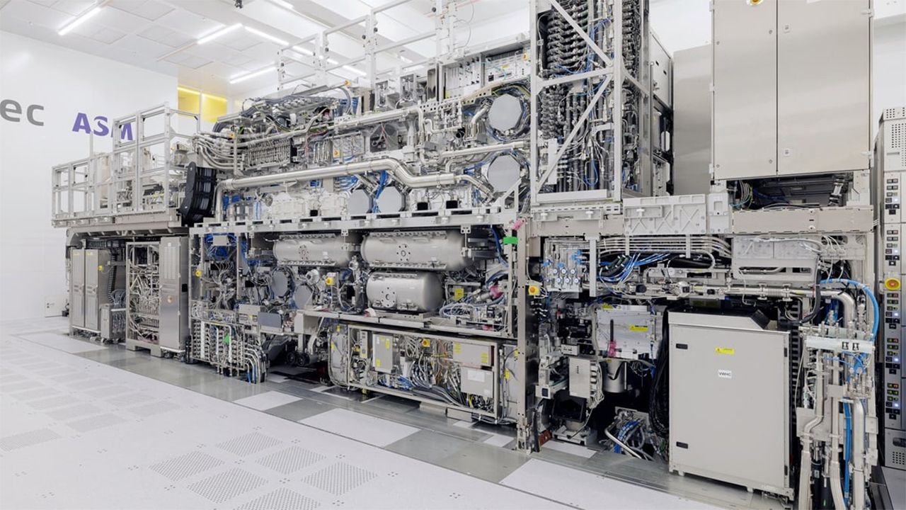
High-NA EUV reduces the single-exposure resolution to 8nm. This leap allows for higher density and cleaner features without the overhead of complex multi-patterning. However, there is a significant trade-off: the "exposure field." Because of the lens geometry required for the 0.55 numerical aperture, High-NA scanners have roughly half the exposure field of current machines.
For companies designing massive AI accelerators, this creates a manufacturing hurdle. A single chip design often spans a larger area than what a single High-NA exposure can cover. Manufacturers are left with two choices: "stitching" multiple exposure fields together or moving to modular, multi-chiplet designs. Both paths present unique challenges regarding power efficiency and throughput. By pushing for 6×12-inch photomasks, TSMC is attempting to solve this geometry problem at the source, allowing for larger, single-die designs that avoid the latency and energy costs associated with chiplet interconnects.
Official Perspectives: The Industry View
The transition to larger 12-inch masks is not a task any single company can accomplish in isolation. It requires a unified effort from EDA vendors, mask manufacturers, and equipment providers. ASML, the sole manufacturer of these advanced scanners, has positioned itself as the catalyst for this industry-wide transformation.
Christophe Fouquet, President and CEO of ASML, emphasized the collaborative nature of this roadmap during a recent briefing. "We expect the adoption of High NA EUV to increase progressively along the device scaling roadmap," Fouquet stated. "We are pleased by the strong initial support of semiconductor manufacturers, mask suppliers, and partners for this initiative. The transition to 12-inch masks is essential to meet the global demand for smaller, faster, and more energy-efficient chips."
The support from the "big three"—TSMC, Intel, and Samsung—suggests that the industry is finally coalescing around a single standard, which is vital for the survival of the High-NA ecosystem. Without such alignment, the costs of re-tooling the global supply chain would be prohibitive for any individual entity.
Implications for the Future of Process Nodes
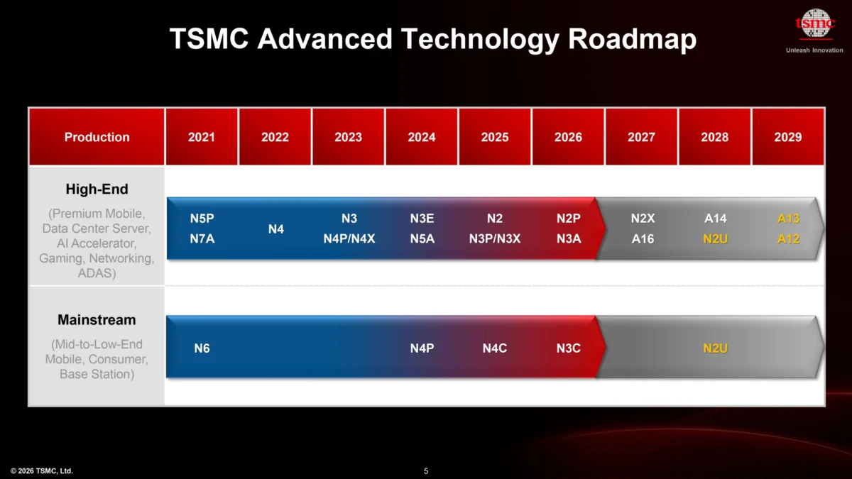
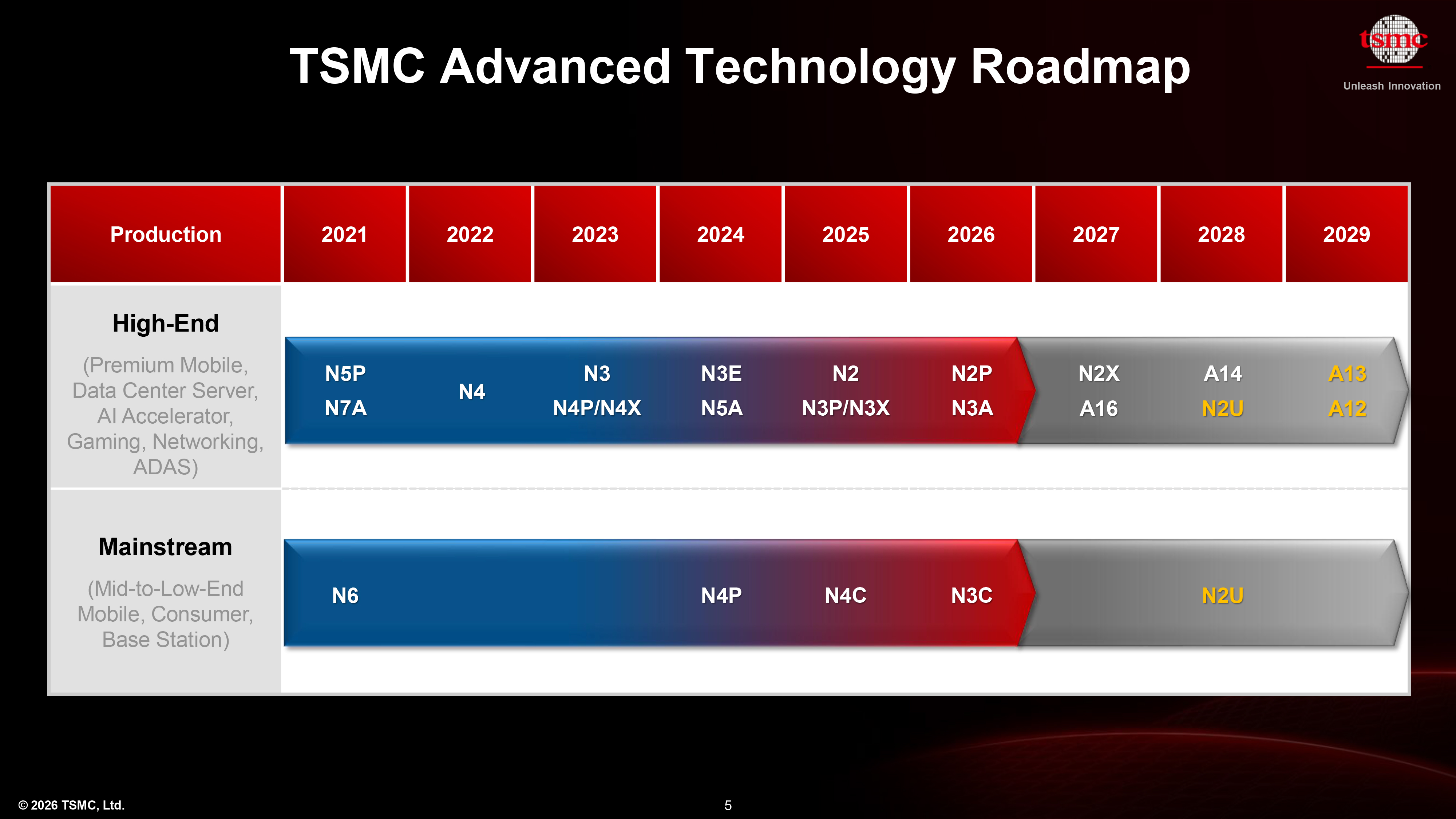
The most pressing question remains: Which process node will be the first to feature this technology? Current roadmaps for TSMC indicate that the A12 and A13 nodes (slated for 2029) will continue to rely on conventional Low-NA EUV. This leaves the 2030 generation—likely to be named A11 or A10 (representing 1.1nm or 1nm-class technology)—as the primary candidates for High-NA integration.
The performance gains expected from these nodes are substantial. With the introduction of 3rd-generation nanosheet GAA transistors, these nodes are projected to deliver significant improvements in power, performance, and area (PPA). If the industry successfully adopts the 12-inch mask standard by 2033, we may see a resurgence in monolithic die design, where the benefits of extreme scaling are combined with the sheer compute capacity of massive, unified processors.
However, the road ahead is fraught with technical risk. The move to High-NA represents the most expensive and complex re-tooling in the history of the semiconductor industry. Everything from the photoresist chemistry to the vibration-dampening systems in the fabs must be recalibrated.
The Broader Impact on Global Technology
As we look toward 2030 and beyond, the implications of TSMC’s announcement extend far beyond the walls of a cleanroom. The move toward High-NA EUV is a foundational pillar for the next generation of artificial intelligence, high-performance computing (HPC), and consumer electronics.
AI accelerators are currently limited by the physical size of the silicon that can be printed in a single pass. As AI models grow in parameter count and complexity, the ability to pack more transistors into a single, high-performance package becomes the primary bottleneck. By enabling 6×12-inch photomasks, TSMC is essentially expanding the "canvas" upon which the world’s most powerful chips are painted.
Furthermore, the transition underscores the intensifying competition in the semiconductor space. By setting a clear timeline for 2030, TSMC is signaling to its customers—such as Apple, NVIDIA, and AMD—that it will maintain its technological lead. It also places pressure on the supply chain to innovate at an unprecedented pace. The semiconductor industry has always been defined by its ability to overcome the impossible, and the leap to High-NA EUV is simply the latest, albeit most expensive, challenge in that ongoing saga.
In conclusion, while the transition to High-NA EUV will be a slow, methodical process, its impact will be seismic. By securing the roadmap for 2030, TSMC has not only clarified its own future but has also provided a sense of stability for the broader tech ecosystem, ensuring that the march toward the atomic scale continues with precision and purpose. Whether or not the industry meets every deadline, the direction is clear: the future of computing will be built on the back of 0.55 numerical aperture lithography.