
 Layla Zulfa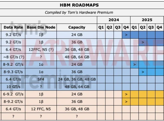
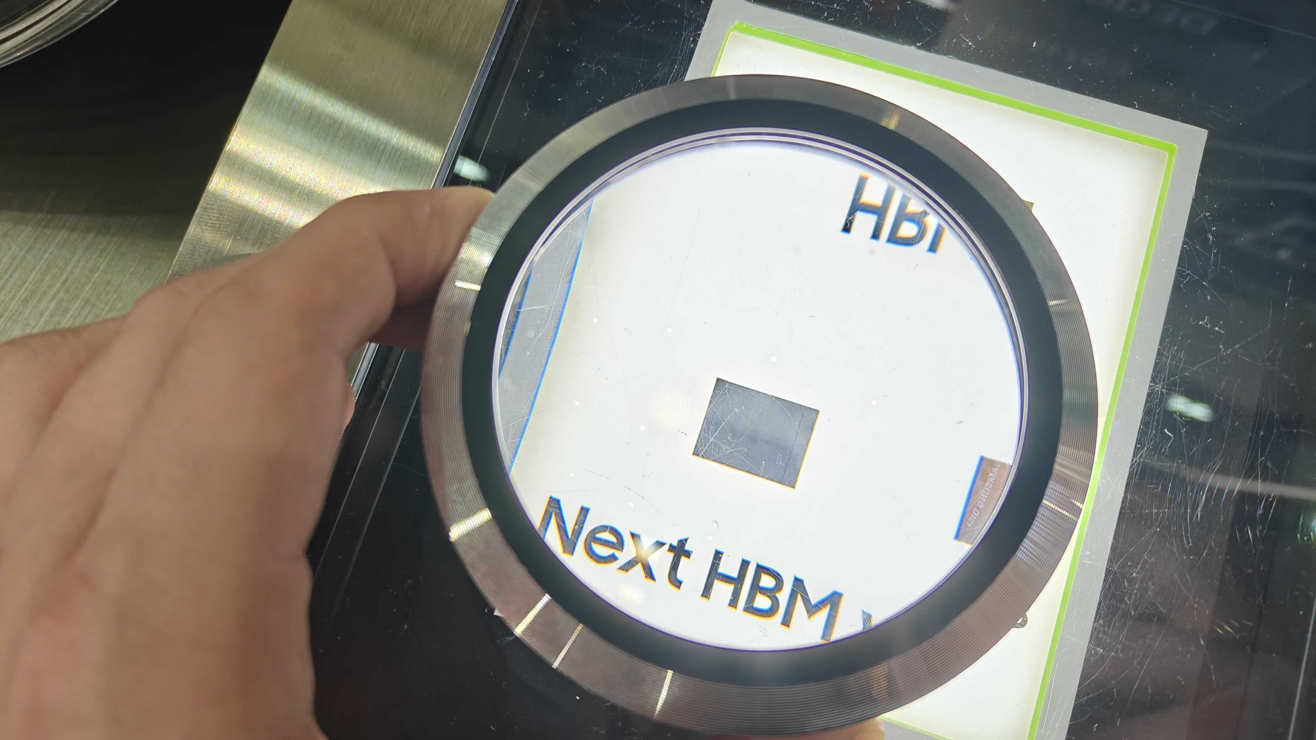
The landscape of High Bandwidth Memory (HBM) is poised for a seismic shift as the industry moves beyond the established standards of the current generation. At the recent "Memory Executive Summit"—a high-profile precursor to the Semicon Taiwan 2026 event—Samsung Electronics unveiled its preliminary vision for HBM5, the next-generation memory architecture. With the relentless demand for AI compute power showing no signs of plateauing, Samsung’s targets are as aggressive as they are necessary: doubling total performance per stack while simultaneously enhancing energy efficiency by 20%.
As the semiconductor industry races to overcome the "memory wall"—the performance bottleneck where memory speed fails to keep pace with GPU and NPU compute capacity—Samsung’s announcement provides a critical, if early, glimpse into how the next three years of hardware development will unfold.
The Core Mandate: Doubling Performance in a Single Generation
The primary headline from Samsung’s announcement, delivered by Choi Jang-seok, head of the product planning team for the memory business division, is the commitment to a twofold increase in bandwidth compared to HBM4E. Achieving this milestone is a monumental engineering challenge. In the world of high-performance computing, where generations are usually marked by incremental gains, a 100% performance jump is highly unconventional.
The Physics of the Bandwidth Problem
To understand the magnitude of this goal, one must look at the math. Current HBM4E standards are projected to operate at approximately 12 GT/s (gigatransfers per second). To double the per-stack bandwidth, engineers are essentially left with three architectural levers:
- Increasing per-pin signaling rates: Pushing speeds toward 24 GT/s.
- Expanding the interface width: Moving from the current 2,048-bit bus to a significantly wider 4,096-bit interface.
- Hybrid Optimization: A combination of moderate clock speed increases and interface widening.
The consensus among industry analysts is that the third option—a hybrid approach—is the most likely path forward. While doubling the pin speed to 24 GT/s would theoretically solve the bandwidth problem, it presents nightmarish signal integrity challenges. Managing power, heat, and timing margins at such speeds requires a drastic overhaul of PHY (Physical Layer) design, which could lead to diminishing returns in terms of power consumption.
Chronology: The Path to HBM5
The trajectory toward HBM5 is not happening in a vacuum. It is the result of a decade of iterative improvements in stacked DRAM.
- 2024–2025: The HBM3E/HBM4 Transition. The industry is currently cementing the HBM4/HBM4E standards. With controllers from firms like Cadence, Rambus, and Synopsys already supporting 16 GT/s, the official JEDEC standards are settling at a conservative 12 GT/s, leaving headroom for proprietary performance extensions.
- 2026: The Planning Phase. Samsung’s announcement at the Memory Executive Summit marks the official start of the industry-wide dialogue for HBM5. Technical specifications are currently being debated in JEDEC committees.
- 2027: Prototyping and Thermal Validation. Development will focus on integrating "Heat Path Blocks" (HPB), which Samsung has already previewed as a solution to thermal resistance.
- 2028–2029: The HBM5 Era. Mass production and integration into AI accelerators are expected to coincide with the next generation of massive-scale AI systems, where 20 to 24 HBM stacks per package become the standard.
Thermal Management: The Heat Path Block (HPB) Innovation
One of the most significant constraints in stacking memory is heat. As HBM stacks grow taller and run faster, the middle layers become increasingly difficult to cool. Samsung’s HBM5 strategy includes the introduction of the Heat Path Block (HPB), a structural optimization designed to reduce thermal resistance by 20%.
By simplifying the cooling architecture, Samsung aims to ensure that the increased bandwidth does not come at the cost of thermal throttling. This is a critical development for the future of AI data centers, where power density is already reaching the limits of traditional air and liquid cooling systems. If Samsung can successfully implement HPB, it will effectively allow for higher, more consistent performance levels without necessitating a radical (and expensive) redesign of server chassis cooling.
Supporting Data: The Scale of Future AI Systems
The urgency for HBM5 is driven by the scaling roadmaps of major AI chip integrators, most notably TSMC. According to recent disclosures from TSMC regarding their CoWoS (Chip-on-Wafer-on-Substrate) roadmap, future AI accelerators are expected to house as many as 24 HBM5/HBM5E stacks within a single system-in-package.
Bandwidth Projections (Per-Stack vs. System)
- HBM4E (Current/Near Future): Estimated at 2 TB/s per stack.
- HBM5 (Target): Projected at 4 TB/s per stack by 2028–2029.
- Total System Bandwidth: With 24 stacks per package, we are looking at a cumulative memory bandwidth of 80 TB/s to 96 TB/s.
This level of bandwidth represents an astronomical leap in data throughput, necessary for training Large Language Models (LLMs) that contain trillions of parameters. Without HBM5, the compute units would spend the vast majority of their cycles idling, waiting for data to traverse the bus.
Engineering Challenges and Trade-offs
While the goal is clear, the implementation is fraught with "engineering traps." Widening the interface to 4,096 bits, as hypothesized by researchers at KAIST and advocated by companies like Marvell, offers a path to higher bandwidth at lower clock speeds. However, this comes with a heavy price:
- Complexity of Routing: A 4,096-bit interface requires double the TSV (Through-Silicon Via) count. This increases the complexity of the base die exponentially.
- Physical Footprint: More I/O paths mean more bumps and more intricate wiring on the interposer, which reduces yield and increases cost per unit.
- Power-per-bit: While lower signaling speeds are generally more energy-efficient (measured in pJ/bit), the sheer number of active drivers and receivers required to support a 4,096-bit bus could negate these gains.
Samsung’s 20% efficiency target implies that they are looking for a "sweet spot"—likely a 3,072-bit interface paired with a moderate, sustainable boost in per-pin signaling. This would represent a balanced compromise between raw throughput and the physical realities of manufacturing at scale.
Implications for the Semiconductor Ecosystem
The shift to HBM5 will have ripple effects across the entire tech industry. For the consumer, it means faster, more capable AI assistants. For the industry, it represents a change in the power dynamics of the semiconductor supply chain.
The Rise of Custom HBM
As memory requirements become more specialized, we are seeing a move away from "one-size-fits-all" memory toward custom HBM solutions. Samsung, Micron, and SK Hynix are all competing to offer the most "integrator-friendly" memory. The HBM5 generation will likely see tighter collaboration between memory makers and GPU designers (like NVIDIA or AMD) earlier in the design cycle.
The "Memory Wall" and Beyond
If the industry successfully achieves these HBM5 targets, it will delay the "memory wall" by at least another five years. However, if HBM5 hits the limits of what is physically possible to cool and route on a silicon interposer, we may see a pivot toward alternative memory architectures, such as optical interconnects or embedded CXL (Compute Express Link) memory pools, which bypass the physical limitations of the package entirely.
Conclusion: A High-Stakes Bet
Samsung’s announcement is not merely a press release; it is a declaration of intent in an increasingly competitive market. By aiming for a doubling of performance and a 20% improvement in energy efficiency, Samsung is setting the bar for the next epoch of high-performance computing.
While the exact specifications of HBM5 remain fluid and subject to the consensus-building processes of the JEDEC standards committee, the direction is unmistakable. We are entering an era where memory bandwidth is no longer a support role for the CPU or GPU—it is the primary driver of progress. Whether through wider interfaces or faster signaling, the innovations emerging from Samsung’s laboratories over the next three years will dictate the capabilities of the artificial intelligence systems of the early 2030s. The path to HBM5 is paved with immense technical hurdles, but the reward—a near-100 TB/s bandwidth ceiling—is the key to unlocking the next generation of digital intelligence.

 Azzam Bilal Chamdy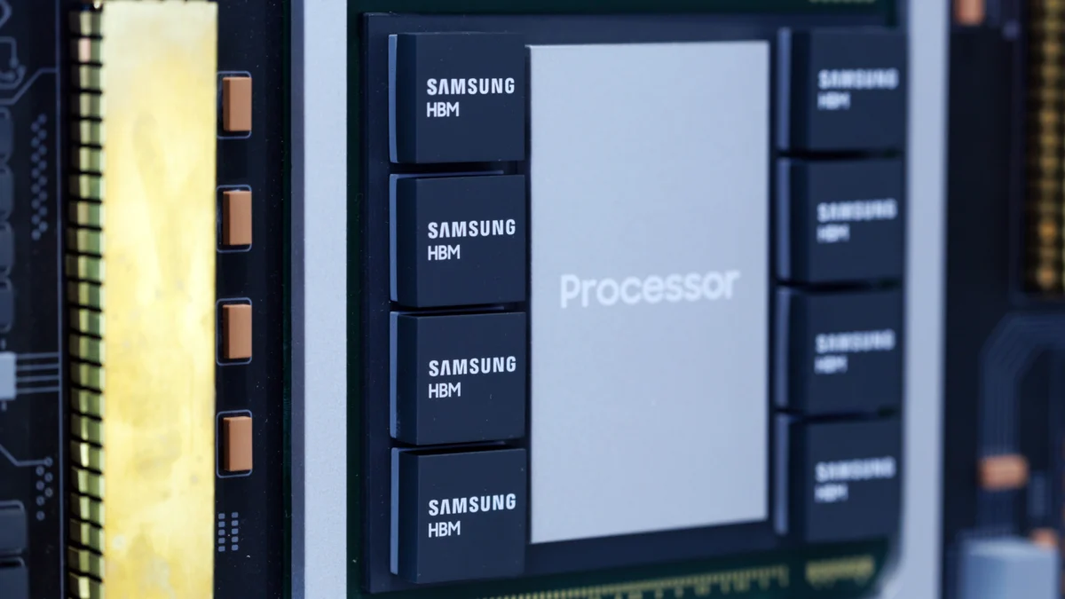
 Muslim