
 Suro Senen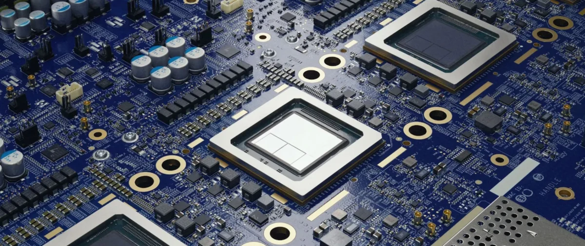
In the high-stakes world of semiconductor engineering, the "blank page" problem is increasingly being solved by silicon-based intelligence. In late August, Architect Labs made waves across the tech industry by announcing the design of a chip developed almost entirely by artificial intelligence—a milestone the firm claims is an industry-first. While AI has long been a staple in the semiconductor toolkit, this development signals a fundamental shift: we are moving from AI as a supportive "copilot" to AI as a primary architect of the very hardware that powers it.
As the semiconductor industry races to meet the insatiable compute demands of generative AI, the design process itself is undergoing a metamorphosis. The industry is transitioning from human engineers using AI to optimize specific sub-tasks toward a future where autonomous agents manage the complex, iterative lifecycle of chip design.
The Main Facts: A New Era of Algorithmic Architecture
For decades, the design of a processor—the "brain" of modern computing—has been a painstaking, manual labor of love, requiring thousands of man-hours to move from RTL (Register Transfer Level) code to a functional, high-yield wafer. Architect Labs’ recent breakthrough suggests that this bottleneck is beginning to dissolve.
The achievement rests on the integration of generative AI into the Electronic Design Automation (EDA) workflow. Historically, EDA tools—the software suites used to design chips—were deterministic and rule-based. Today, these tools are being imbued with machine learning and agentic capabilities. An agentic system does not simply follow a command; it evaluates a problem, proposes a design iteration, simulates the result, detects inefficiencies, and modifies the design autonomously.
By leveraging these systems, Architect Labs has demonstrated that the iterative loop of "design-simulate-verify" can be accelerated by orders of magnitude. The result is a hardware architecture that is not only faster to produce but potentially optimized in ways that human intuition might miss, particularly in the realm of signal integrity, power distribution, and thermal management.
A Chronology of Silicon Evolution: From CAD to Autonomous Agents
To understand the magnitude of this shift, one must look at the evolution of chip design over the last half-century.
The Era of Manual Drafting (1970s–1980s)
In the early days of microprocessors, engineers relied on physical layouts and rudimentary software to draw circuits. Every transistor was meticulously placed, and logic errors were often only discovered during the physical manufacturing phase, leading to costly re-spins.
The Rise of Automation (1990s–2010s)
The introduction of sophisticated EDA software from companies like Cadence, Synopsys, and Siemens (Mentor Graphics) allowed for the automation of "placement and routing." During this period, AI made its first appearance, primarily in the form of heuristic algorithms used to optimize floorplans and verify logic gates. It was a partnership of human creativity and computer-aided precision.
The Generative Threshold (2020–2023)
The advent of Large Language Models (LLMs) and advanced reinforcement learning marked the next phase. Engineers began using AI to assist in writing Verilog and VHDL code. These models could scan millions of lines of code to identify potential bugs, effectively acting as an automated "spell-check" for silicon architecture.
The Agentic Milestone (2024–Present)
The announcement from Architect Labs in August 2024 represents the current zenith: the emergence of "Agentic EDA." These systems no longer wait for human prompts for every micro-adjustment. They operate within set constraints to achieve an objective, such as "maximize clock speed while keeping power consumption below 5 watts," and iterate through thousands of architectural permutations before presenting the best options to human supervisors.
Supporting Data: The Complexity Crisis and the AI Solution
The necessity of this shift is driven by the "Complexity Crisis." As Moore’s Law encounters physical limitations, packing more transistors into a smaller footprint requires exponentially more complex layouts.
- Design Time Reduction: Industry analysts suggest that transitioning to AI-assisted design can reduce the "Time-to-Tapeout" by 20% to 40%. In a market where being six months late can result in the loss of billions in potential revenue, this is a competitive imperative.
- Performance Metrics: Preliminary data indicates that AI-optimized floorplans can yield a 5% to 10% improvement in power efficiency compared to human-only designs. While 5% might sound marginal to a layperson, in data center-scale operations, it translates to millions of dollars in energy savings annually.
- Verification Efficiency: Verification typically consumes 60% to 70% of a chip development project’s timeline. Agentic AI tools are proving highly effective at creating "test benches"—automated environments that stress-test chips under billions of scenarios—vastly exceeding the capacity of human QA teams.
Despite these figures, human oversight remains critical. Current AI systems struggle with "global strategy"—the high-level vision of what a chip is meant to do. AI excels at micro-optimization, but the macro-architecture still requires the nuanced understanding of a human architect.
Official Responses and Industry Perspectives
The reaction from the semiconductor ecosystem has been a mix of excitement and measured caution.
"We are seeing the democratization of silicon," says a representative from a leading EDA software firm. "By lowering the barrier to entry for complex chip design, AI allows smaller startups to compete with industry giants. However, we must be wary of ‘black box’ designs where the AI makes an optimization that a human engineer cannot explain. If we cannot explain the architecture, we cannot guarantee its long-term reliability."
Researchers at UC Berkeley, who have been monitoring the integration of LLMs into chip design, emphasize that we are not yet at the stage of "lights-out" manufacturing. "AI is out-designing human engineers in narrow, highly technical areas," says a lead researcher in the field. "But when you zoom out to system-level architecture, the human role as the ultimate arbiter remains indispensable. The AI is a powerful tool, but it lacks the strategic intent to pivot a product based on market trends or unique application-specific needs."
Architect Labs, for their part, maintains that their breakthrough is intended to empower, not replace, the workforce. "Our goal is to allow engineers to focus on the ‘what’ and the ‘why,’ leaving the ‘how’—the tedious, repetitive, and computationally heavy lifting—to our AI systems," the company noted in their blog post.
Implications: The Recursive Feedback Loop
Perhaps the most profound implication of this technological shift is the recursive nature of the relationship between AI and silicon.
The Hardware-Software Symbiosis
We are currently in a feedback loop:
- Human-designed processors run AI training models.
- AI models assist in designing more powerful, efficient processors.
- The new processors enable more advanced AI models.
This "recursive acceleration" could shorten the cycles of technological innovation to a point where human-led R&D cycles appear stagnant. As AI takes more control over the hardware it runs on, we may see the emergence of chips optimized for the specific "thought patterns" of future neural networks—hardware that is evolved rather than traditional engineering.
The Talent Shift
The skill set of a chip engineer is fundamentally changing. The engineer of 2030 will likely be less of a layout technician and more of a "Silicon Architect-Curator." They will need to understand prompt engineering, machine learning optimization, and the ethics of autonomous design, while maintaining a firm grasp on the laws of physics that govern semiconductor behavior.
Security and Reliability
A major implication of AI-designed hardware is the question of security. If an AI writes the RTL code for a processor, how do we ensure there are no "hidden" vulnerabilities or backdoors? The industry will need to develop new standards for "AI-Assisted Verification," where a second, independent AI system is tasked with auditing the work of the first, creating a "red team" vs. "blue team" dynamic in silicon design.
Conclusion: The Horizon of Autonomous Silicon
The Architect Labs announcement marks a significant milestone in the history of computing. We have moved from the era of manual calculation to the era of machine-assisted design, and now, to the cusp of autonomous architectural creation.
While the "Silicon Autopilot" is not yet ready to take full control—and indeed, should not be allowed to do so without rigorous human oversight—it is clear that the future of semiconductor development is inextricably linked to the capabilities of AI. As we move forward, the most successful companies will be those that strike the right balance between the raw, iterative speed of autonomous agents and the strategic, visionary foresight of human engineers.
The chip of the future will be more powerful, more efficient, and more complex than anything we have seen to date. And in a fitting turn of events, it will be a chip that effectively designed itself, built by the very intelligence it was created to host. The feedback loop is closed, and the acceleration has only just begun.

 Nana Wu
 Sagoh
Sagoh