
In a move that underscores the escalating arms race for semiconductor supremacy, South Korean memory giant SK Hynix has unveiled an unprecedented long-term investment strategy that promises to reshape the global landscape of 3D NAND and High-Bandwidth Memory (HBM) production. The company has announced an initial injection of KRW 100 trillion ($64 billion) into its Cheongju campus, but this represents only a fraction of a staggering $712.5 billion (KRW 1.1 quadrillion) commitment aimed at solidifying South Korea as the undisputed epicenter of the world’s memory manufacturing.
This strategic pivot comes at a critical juncture for the tech industry, as the surge in artificial intelligence (AI) and machine learning workloads continues to drive an insatiable demand for high-performance memory. By positioning its massive infrastructure projects for the coming decades, SK Hynix is not merely expanding capacity—it is building the foundation for the next era of computing.
The Cheongju Expansion: A Hub for Future Memory
The most immediate piece of this grand puzzle is the $64 billion investment in the Cheongju campus. This site, which has historically served as a cornerstone of SK Hynix’s 3D NAND flash memory production, is set to undergo a significant evolution.
Under the new development roadmap, the company plans to construct the "M17" fabrication facility. With construction slated to begin in 2025, the facility is expected to reach operational status by 2029. The capital expenditure is divided into two primary tranches: roughly $51.8 billion (KRW 80 trillion) dedicated to the construction and equipment of the 3D NAND fab, and approximately $12.9 billion (KRW 20 trillion) earmarked for the P&T7 packaging and test facility.
This integration is vital. As the industry moves toward more complex 3D NAND structures and the increasingly critical HBM stack, the proximity of manufacturing to advanced back-end packaging becomes a decisive competitive advantage. By consolidating these functions at the Cheongju site, SK Hynix aims to streamline production cycles and accelerate time-to-market for its high-margin memory products.
Chronology: A Roadmap to 2033 and Beyond
The scale of SK Hynix’s ambition is best viewed through its projected timeline. The company’s roadmap is structured to ensure a continuous ramp-up of production capability, mitigating the risk of supply chain bottlenecks while keeping pace with the exponential growth of the AI hardware market.
- 2025: Commencement of construction for the M17 fab at the Cheongju site.
- 2027: The first facility at the Yongin Semiconductor Cluster is expected to go online, marking the beginning of a massive surge in DRAM output.
- 2028–2029: The M17 fab at Cheongju reaches operational maturity, significantly boosting 3D NAND and HBM assembly capacity.
- 2033: The target date for the completion of all four fabs within the Yongin Semiconductor Cluster, a timeline accelerated by over a decade from original projections.
- 2035 and beyond: Continued phased development of the Southwestern Semiconductor Cluster, with long-term infrastructure maturation and capacity expansion.
This aggressive timeline is necessitated by the lead times required for semiconductor infrastructure. As evidenced by the development of the Yongin cluster, which took nine years to conceptualize and initiate, planning must occur nearly a decade in advance to accommodate power, water, and logistical requirements.
Supporting Data: The Yongin and Southwestern Clusters
While the Cheongju investment is substantial, it is eclipsed by the company’s plans for the Yongin Semiconductor Cluster and the yet-to-be-sited Southwestern Semiconductor Cluster.

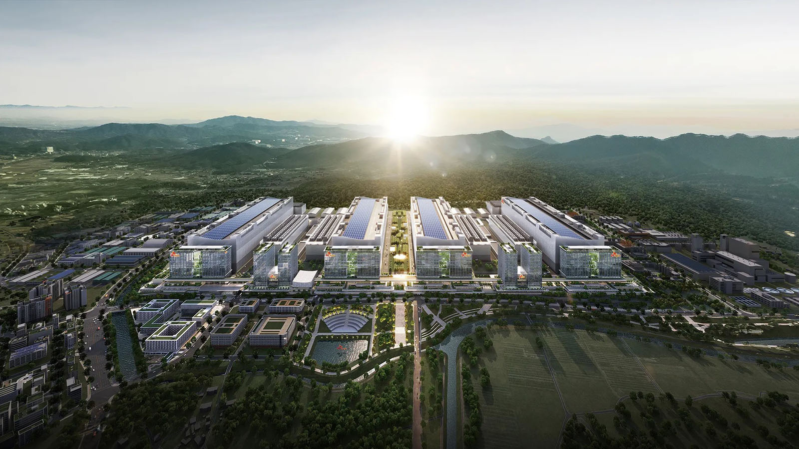
The Yongin Semiconductor Cluster ($389.3 Billion)
The Yongin project stands as the largest single investment commitment in the company’s history. Once a greenfield site, it is being transformed into a sprawling manufacturing hub designed to be the company’s flagship DRAM production center. By condensing the construction timeline for the site’s four planned fabs—now targeting completion by 2033—SK Hynix is signaling a massive bet on the sustained dominance of DRAM in the AI ecosystem.
The Southwestern Semiconductor Cluster ($259.5 Billion)
Perhaps the most ambitious component is the planned Southwestern cluster. Unlike the other sites, this project is currently in the site-selection phase. SK Hynix is working closely with the South Korean central and local governments to evaluate the viability of various regions based on critical infrastructure metrics: electricity grid stability, water supply capacity, transportation networks, and long-term land availability. This cluster is envisioned as the successor to the company’s existing hubs in Icheon, Cheongju, and Yongin, serving as a future-proofed base for the next generation of semiconductor manufacturing.
Official Responses and Strategic Rationale
SK Hynix’s official messaging emphasizes the necessity of these investments as a response to global market volatility and the "AI Supercycle." In official statements, the company has characterized these investments as a proactive measure to ensure the long-term sustainability of the global memory supply chain.
"The development of new semiconductor clusters is a multi-generational effort," an SK Hynix representative noted. "By securing the necessary infrastructure today—including massive commitments to energy and water—we are creating an ecosystem that will remain the bedrock of the global tech economy for the next several decades."
The South Korean government has largely welcomed these plans, viewing them as a crucial component of the nation’s economic security strategy. By fostering a domestic semiconductor "super-cluster," the government aims to insulate the Korean economy from global trade tensions while maintaining its technological lead over competitors.
Competitive Landscape: The Chungcheong Region Arms Race
SK Hynix is not acting in a vacuum. The announcement of its investment plan was closely followed by Samsung’s own disclosure of a KRW 140 trillion ($90.98 billion) investment in the Chungcheong region.
This rivalry is driving an unprecedented level of industrial development in South Korea. Samsung’s plan focuses on diversifying its reach within the semiconductor and display sectors:
- Display: Expansion of OLED production in Asan.
- Memory: Construction of five new HBM production lines in Onyang, alongside modernization efforts in Cheonan.
- Battery Technology: Establishment of a pilot production line for next-generation battery technologies in Cheonan.
- Advanced Packaging: Expansion of AI server package substrate manufacturing in Sejong.
The concentration of these massive investments in the same geographic region suggests that both companies are competing to attract the same pool of specialized talent and infrastructure support, further cementing South Korea’s status as a global powerhouse.
Implications: What This Means for the Industry
The ramifications of these investments will be felt across the entire electronics supply chain for years to come.
1. Market Stability vs. Oversupply
While the primary goal of these investments is to meet future demand, they also serve as a deterrent to competitors. By promising massive capacity, SK Hynix and Samsung are setting a "floor" for the industry, ensuring that they can achieve economies of scale that smaller or less well-funded competitors will find difficult to match. However, there is a lingering concern among market analysts regarding the potential for cyclical oversupply if the AI demand surge ever plateaus.
2. The Dominance of HBM and Advanced Packaging
The specific focus on HBM packaging at both the Cheongju and Onyang sites highlights the industry’s shift away from generic memory toward specialized, high-performance components. As AI chips (like those from NVIDIA and AMD) become more reliant on HBM, the manufacturers who control the most efficient packaging processes will effectively hold the keys to the kingdom.
3. Energy and Infrastructure Demands
The sheer scale of these projects brings the issue of power consumption to the forefront. These clusters require an astronomical amount of electricity and water. The successful implementation of these plans will depend heavily on the ability of the South Korean government to upgrade the national power grid and water infrastructure, potentially fueling a secondary wave of investment in green energy and sustainable utility management.
4. Geopolitical Positioning
In an era of "onshoring" and "friend-shoring," these massive domestic investments serve a strategic purpose. By keeping their most advanced fabrication facilities within South Korea, SK Hynix and Samsung are mitigating the risks associated with global supply chain disruptions and political instability. This is a clear signal to the rest of the world that South Korea intends to remain the primary, most reliable source of advanced semiconductor components.
Conclusion
The $712.5 billion investment plan by SK Hynix is more than just a capital expenditure report; it is a statement of intent. By looking past the immediate market fluctuations and focusing on a multi-decade expansion, the company is positioning itself to be the primary engine of the AI-driven future. While the path to completion involves massive logistical, technical, and environmental hurdles, the scale of this commitment ensures that the global semiconductor industry will remain anchored in the Korean peninsula for the foreseeable future. As the world moves deeper into the era of artificial intelligence, the memory produced within these new, sprawling clusters will likely power everything from the servers of the largest tech conglomerates to the devices in our pockets.