The landscape of high-performance computing is undergoing a seismic shift. As the global demand for data-intensive processing—driven by the rapid expansion of artificial intelligence (AI), machine learning, 5G telecommunications, and the burgeoning "metaverse"—reaches a fever pitch, the fundamental architecture of memory technology is struggling to keep pace. Addressing this bottleneck, Samsung Electronics has officially commenced mass production of the industry’s smallest and most advanced 14nm Extreme Ultraviolet (EUV) DDR5 DRAM. This milestone not only cements Samsung’s leadership in the semiconductor sector but also provides the necessary bandwidth and power efficiency to power the next generation of digital infrastructure.
A Legacy of Innovation: The Road to 14nm EUV
To understand the magnitude of this announcement, one must look at the chronology of Samsung’s semiconductor advancements. In 2020, Samsung achieved a historic industry first by successfully shipping EUV-based DRAM. This was the opening salvo in a war against the physical limitations of lithography. Prior to the integration of EUV technology, DRAM manufacturers relied on ArF (Argon Fluoride) immersion lithography, which faced increasing difficulty in patterning smaller circuits without introducing defects.
By transitioning to EUV lithography—a process that uses shorter wavelengths of light to etch ultra-fine circuit patterns onto silicon wafers—Samsung effectively bypassed the traditional scaling walls. The 2020 rollout served as the proof of concept. Having validated the stability and yield of the EUV process, Samsung spent the intervening months refining its 14nm node. Today, the mass production of 14nm EUV DRAM represents the culmination of this intense research and development phase. It marks the shift from experimental implementation to widespread industrial application, setting a new benchmark for "five-layer" EUV integration, which allows for the highest density of any DRAM currently in production.
Technical Specifications: Pushing the Boundaries of Physics
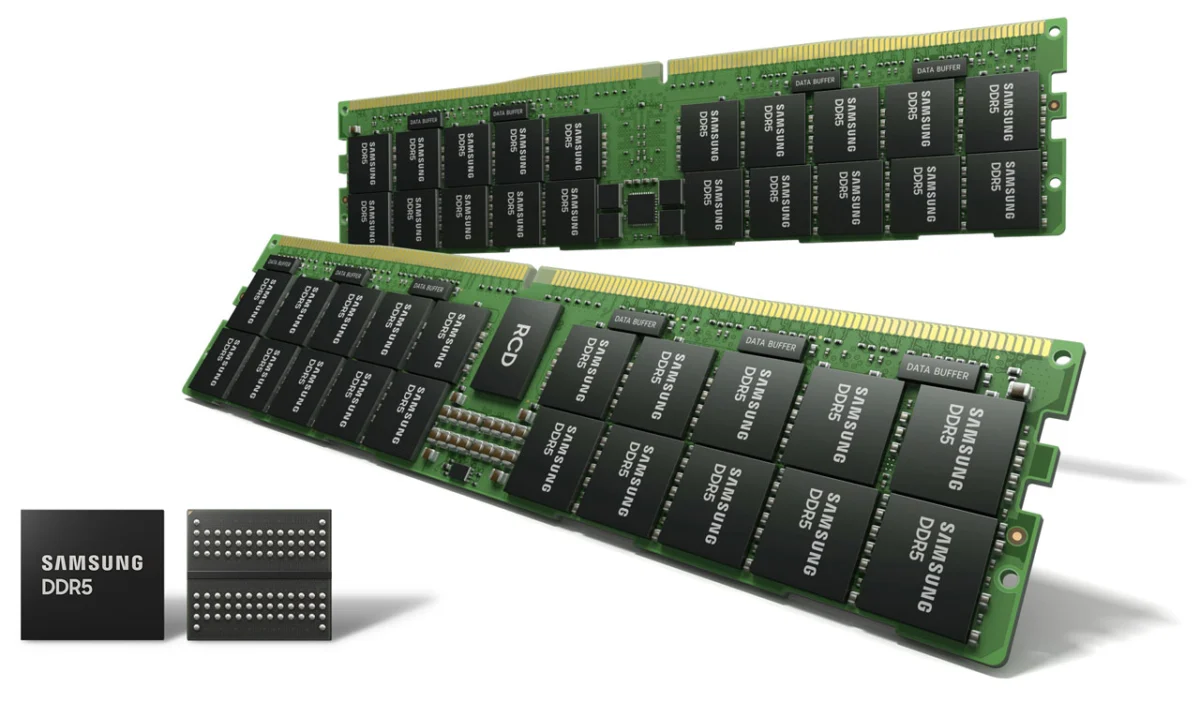
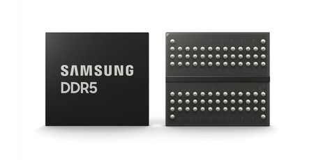
The technical implications of Samsung’s latest 14nm DDR5 modules are profound. By leveraging the industry-leading 14nm node, Samsung has managed to cram significantly more transistors into a smaller surface area, resulting in a DRAM architecture that is simultaneously more capacious and more efficient.
Performance Benchmarks
According to internal testing conducted by Samsung, the new 14nm DDR5 DRAM offers a 20 percent improvement in overall productivity compared to the previous generation of memory. This is not a marginal gain; in the context of data centers and high-end workstations, a 20 percent increase in throughput can translate to massive reductions in processing time for complex AI modeling and real-time data analytics.
The leap in raw speed is equally impressive. While the current DDR4 standard typically operates at a reliable 3.2Gbps, Samsung’s new DDR5 standard is engineered to achieve speeds of up to 7.2Gbps. This more than doubles the data rate, providing the "bandwidth headroom" required by modern CPUs to prevent the memory-bound performance bottlenecks that have plagued high-core-count processors in recent years.
Power Efficiency
In an era where sustainability and power consumption are critical metrics for data center operators, the 14nm process offers a 20 percent improvement in energy efficiency. As energy costs fluctuate and environmental regulations tighten, the ability to deliver more computational power per watt is a primary competitive advantage for the hyperscale cloud providers who will be the primary consumers of these high-capacity modules.
Official Perspectives: The Vision for a Data-Driven World
The weight of this announcement was underscored by Jooyoung Lee, Senior Vice President and Head of the DRAM Product & Technology team at Samsung Electronics. In an official press statement, Lee characterized the development as a "critical milestone" in the history of memory scaling.
"Our 14nm EUV technology is the result of years of overcoming the physical limitations of traditional semiconductor patterning," Lee noted. He emphasized that the primary goal of this innovation is to support the "data-driven world." Samsung’s strategic vision is clear: as AI and the metaverse transition from buzzwords to functional, real-world utility, the hardware foundation must be capable of processing petabytes of information with near-zero latency. By prioritizing extreme miniaturization, Samsung is positioning itself as the indispensable architect of this new digital reality.
The Future Roadmap: Scaling to 24Gb and Beyond
While the current mass production focuses on standard capacities, Samsung has already signaled its intent to push the boundaries of IC density. The company plans to refine its 14nm process to increase individual integrated circuit (IC) density to 24Gb.
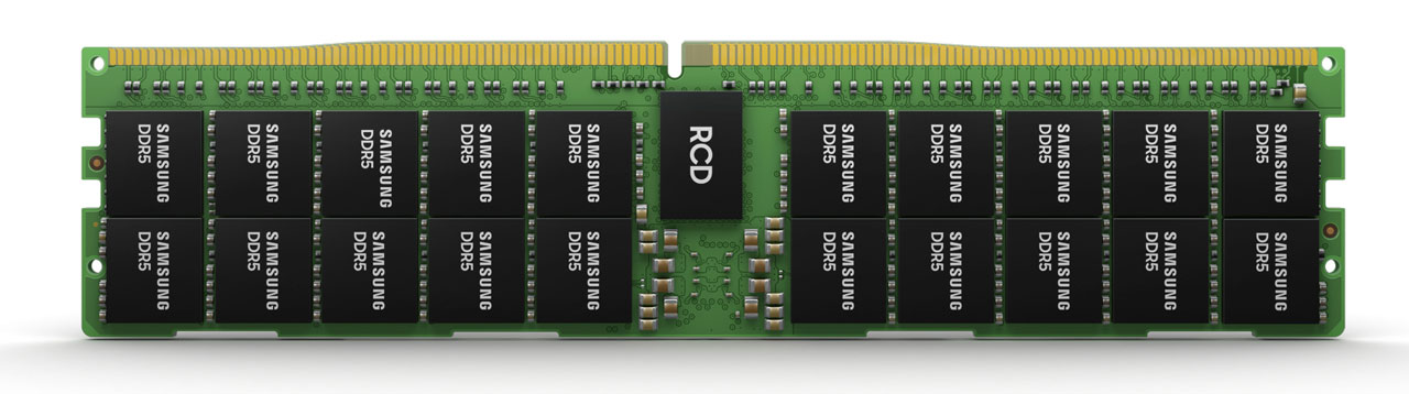
The ramifications of this are substantial for the workstation and server markets. By utilizing 24Gb dies, manufacturers can produce massive 768GB DDR5 DIMMs. This level of memory density would allow for server configurations that were previously impossible, enabling in-memory databases and large-scale virtualization projects that require massive amounts of active, high-speed RAM. While mainstream consumer DIMMs are expected to stay in the 64GB-per-stick range initially, the path toward ultra-high-capacity memory is now clearly paved.
Market Implications: The Cost of Early Adoption
Despite the excitement surrounding DDR5, the transition period presents a complex challenge for both system builders and consumers. New hardware standards rarely come without a "premium" tax, and the launch of DDR5 is no exception.
The Motherboard Dilemma
Industry observers have noted that motherboard manufacturers are taking a cautious approach to the transition. Recent leaks, including the registration of Asus Prime Z690 series boards with "D4" suffixes, indicate that motherboard vendors are hedging their bets by offering dual-path support. By producing variants that support either DDR4 or DDR5, these companies are attempting to lower the barrier to entry for users who want the latest CPU performance (such as Intel’s Alder Lake-S) without being forced to pay the inflated costs of initial DDR5 production.
The Pricing Reality
The cost of early adoption is currently quite high. Recent listings on retailers like Newegg and international equivalents have provided a sobering reality check for enthusiasts. A 32GB (2 x 16GB) kit of GeIL Polaris RGB DDR5-4800 memory was spotted with a retail price tag of approximately $349.99 USD. Equivalent listings in international markets, such as Japan, show similar trends, with pricing converting to between £250 and £300.
For the average consumer, this represents a significant increase in build costs compared to the mature DDR4 market, where 32GB kits have become increasingly affordable. This price disparity suggests that for the next 12 to 18 months, DDR5 will remain a "prosumer" and enterprise-grade technology. The cost is expected to stabilize as yields improve and Samsung’s mass-production pipeline hits full capacity, but until then, builders will have to weigh the performance benefits of 7.2Gbps speeds against the steep initial investment.
Conclusion: A Fundamental Shift in Architecture
Samsung’s advancement to 14nm EUV DRAM is more than just a news item regarding faster RAM; it is a clear indicator of where the tech industry is headed. The ability to shrink components while simultaneously increasing speed and efficiency is the heartbeat of technological progress.
As we look toward the mid-2020s, the integration of 14nm EUV technology will likely become the standard for all high-end computing. While the initial costs may deter the casual builder, the enterprise sector will undoubtedly embrace this transition as a necessary evolution to support the next wave of AI, 5G, and metaverse applications. Samsung has fired the starting gun on a new race for memory dominance, and the rest of the industry is now scrambling to keep pace. Whether this leads to a rapid price correction or a prolonged period of premium hardware pricing remains to be seen, but one thing is certain: the future of computing will be built on the back of this tiny, EUV-patterned silicon.