 Azzam Bilal Chamdy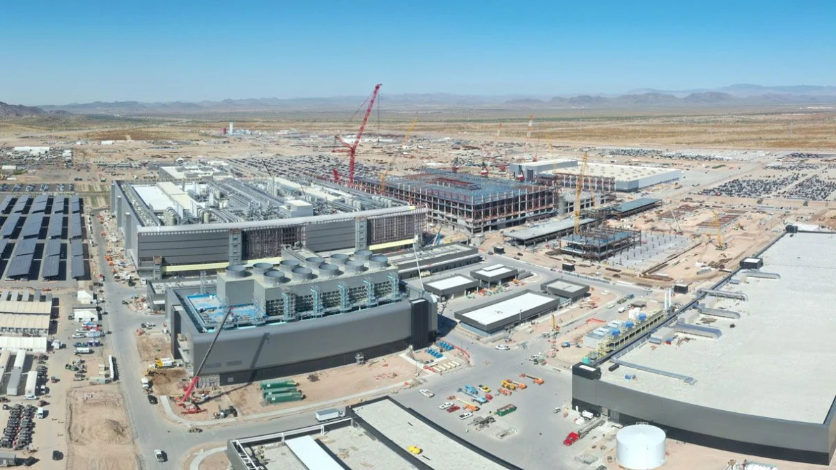
In the race for global technological supremacy, the narrative of "onshoring" has become the centerpiece of industrial policy. In recent weeks, industry titans Nvidia and Intel have engaged in a high-stakes rhetorical exercise, painting a picture of a revitalized American semiconductor landscape. By leveraging federal incentives and a robust network of domestic partners, these companies claim to be insulating the United States from the volatile vulnerabilities of the global supply chain.
However, beneath the glossy surface of press releases and "America 250" branding lies a more complex, nuanced, and perhaps sobering reality. While the architecture of an American chip industry is indeed rising, the actual path from raw wafer to functional AI accelerator remains largely tethered to international hubs. The dream of a fully self-contained U.S. AI supply chain is, for now, a project in progress, not a fait accompli.
Main Facts: The New Semiconductor Geography
Nvidia’s recent corporate communications are bold in their scope. The company asserts that its manufacturing and supply chain footprint now spans 43 states, effectively turning the U.S. into a sprawling, interconnected factory floor. The centerpiece of this narrative is TSMC’s Phoenix, Arizona facility, which has officially begun producing Blackwell-class wafers at volume.
Nvidia has projected a staggering $500 billion investment in AI infrastructure over the next four years, executed in tandem with a coalition of industrial heavyweights: TSMC, Foxconn, Wistron, Corning, Coherent, and Amkor. This consortium is intended to create a closed-loop system capable of meeting the insatiable demand for AI compute.
Simultaneously, Intel has launched its own initiative, titled "America 250," which emphasizes the company’s unique position as an integrated device manufacturer (IDM). Intel argues that it provides a rare end-to-end U.S. capability—from the initial architectural design to the final stages of advanced packaging—positioning itself as the primary safeguard for American technological sovereignty.
Yet, a critical analysis of these claims reveals a systemic "missing link." While the front-end fabrication—the creation of the silicon wafers themselves—is successfully migrating to Arizona, the process stops there. Every Blackwell die produced in the desert Southwest must still cross the Pacific Ocean to be packaged. Furthermore, the high-bandwidth memory (HBM) essential to these chips is neither manufactured nor packaged within the United States. These gaps are not merely logistical inconveniences; they are structural dependencies that define the current limitations of domestic semiconductor autonomy.
Chronology: The Road to 2028 and Beyond
The current state of affairs is the result of decades of strategic offshoring, and the reversal of this trend is a multi-year, multi-billion-dollar endeavor.
- 2020-2022 (The Realization): Supply chain disruptions during the COVID-19 pandemic exposed the fragility of a globalized semiconductor model. The U.S. government responded with the CHIPS and Science Act, providing the legislative framework to incentivize domestic investment.
- 2023-2024 (The Fabrication Build-out): TSMC’s Arizona facility (Fab 21) reaches a major milestone by successfully transitioning to the production of high-performance Blackwell wafers. Nvidia formalizes its partnerships with domestic suppliers, diversifying its sourcing across 43 states.
- 2025-2026 (The Packaging Pivot): The current period is defined by the reliance on Asian packaging facilities, specifically those using CoWoS (Chip-on-Wafer-on-Substrate) technology. Companies like Amkor are beginning to invest in U.S. packaging capacity, but these facilities remain in the construction or pilot phase.
- 2027 (The Testing Phase): Industry analysts anticipate that localized assembly and test (OSAT) services will begin to scale, though they will likely handle only a fraction of the total Blackwell output.
- 2028 (The Target Horizon): According to current projections, the first major domestic facilities capable of closing the loop—handling advanced packaging and potentially integrating HBM—are slated to come online. This year serves as the "North Star" for the industry’s goal of achieving a truly domestic AI supply chain.
Supporting Data: The Anatomy of a Supply Chain Gap
The disparity between "Made in the USA" branding and manufacturing reality can be quantified by the complexity of the semiconductor lifecycle.
Front-End Fabrication
The transition of front-end fabrication (the etching of transistors onto wafers) to the U.S. is the most successful element of the current strategy. TSMC’s Arizona investment is a testament to this, with high-volume production of advanced nodes now a reality. This accounts for roughly 40-50% of the total chip manufacturing effort.
The Packaging Bottleneck
Advanced packaging, particularly for AI GPUs, is arguably the most critical and complex step in modern chip design. It involves connecting multiple dies (compute, HBM, I/O) on a high-speed interposer. Currently, this process is almost exclusively performed in Taiwan, leveraging the high-density interconnect capabilities of CoWoS. The lack of this infrastructure in the U.S. means that even a "Made in Arizona" chip is fundamentally unfinished until it returns from an overseas facility.
The Memory Deficit
HBM is the third pillar of the AI hardware triad. The production of HBM is highly concentrated in South Korea (dominated by SK Hynix and Samsung) and parts of Taiwan. There is currently zero domestic HBM production capacity in the U.S. The specialized equipment and the "stacking" expertise required for HBM represent a technological moat that will take years for U.S.-based partners to bridge.
Official Responses: Managing Expectations
When pressed on these gaps, industry leaders typically point to the "ecosystem" approach. Nvidia’s leadership has frequently emphasized that they are building a "network of partners," not a single factory. They argue that the geographic dispersal of the supply chain is a feature, not a bug, designed to ensure that no single region is a point of total failure.
Intel, for its part, maintains that its internal vertical integration is the answer. Their "America 250" rhetoric focuses on their internal foundry services (IFS) and their ongoing expansion of advanced packaging facilities in New Mexico and Ohio. Intel executives argue that while the industry is currently fragmented, their long-term roadmap provides the only path toward true sovereignty.
However, independent analysts remain cautious. They suggest that these "official responses" often elide the distinction between starting a project and achieving scale. The capital expenditure required for packaging facilities is enormous, and the workforce training required to operate these facilities at the necessary precision levels remains a significant barrier to entry.
Implications: Strategic Vulnerability vs. Industrial Progress
The implications of this ongoing transition are profound, both geopolitically and economically.
1. The Geopolitical Risk
So long as the Blackwell dies must transit the Pacific for packaging, the U.S. AI industry remains inherently linked to the stability of the Taiwan Strait. Any disruption in the logistics chain—whether through natural disaster, geopolitical conflict, or maritime trade restrictions—would immediately halt the production of the world’s most advanced AI models.
2. The Economic Multiplier
The $500 billion investment mentioned by Nvidia is not just a cost; it is an economic stimulus package. The construction of fabs, packaging centers, and the associated supply chain infrastructure is creating thousands of high-skilled manufacturing jobs. The long-term economic benefit of having a localized semiconductor ecosystem cannot be overstated, even if the "total independence" goal remains several years away.
3. The Innovation Bottleneck
Innovation moves at the speed of the supply chain. When a design team in California has to wait weeks for a chip to be packaged in Asia, the "loop of iteration"—the time it takes to test, refine, and improve a design—is artificially lengthened. Establishing packaging and HBM production on U.S. soil will likely accelerate the pace of AI innovation by orders of magnitude, turning months-long feedback cycles into weeks.
Conclusion
The narrative presented by Nvidia and Intel is not a falsehood, but it is an incomplete picture. We are currently witnessing the "Fabrication Age" of American semiconductor resurgence. The "Packaging and Memory Age" is still in its infancy.
By 2028, the industry hopes to have closed these gaps, creating a genuinely self-sustaining American AI supply chain. Until then, the "Made in the USA" label on our most advanced AI hardware will carry an asterisk. The progress made thus far is historic, but the most difficult engineering and logistical challenges lie ahead. For policymakers and investors alike, the next four years will be the definitive test of whether the promise of domestic autonomy can survive the reality of globalized dependencies.


 Dwi Wanna
 Siti Muinah