
In the relentless pursuit of higher computational performance, the semiconductor industry has hit a thermal wall. As AI-driven workloads demand increasingly dense transistor counts and higher clock speeds, the heat generated by these silicon behemoths has become the primary bottleneck for further innovation. Now, a breakthrough from Diamond Foundry—a leader in lab-grown diamond technology—promises to fundamentally change the way we manage heat in high-performance computing.
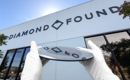
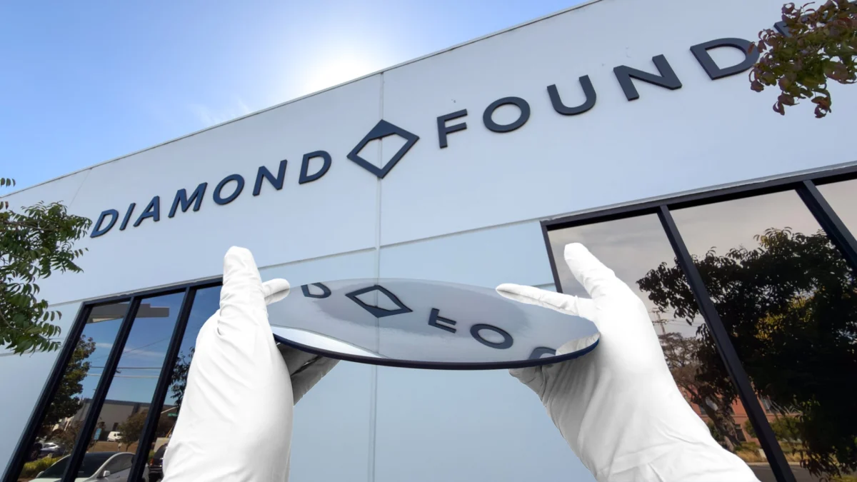
The company has officially unveiled the world’s first 200mm single-crystal diamond (SCD) wafer. By successfully scaling diamond manufacturing to the standard dimensions used by semiconductor foundries, Diamond Foundry has effectively signaled that the “diamond era” of electronics cooling is no longer a theoretical pursuit, but a manufacturing reality.
The Main Facts: Why Diamond?
To understand the magnitude of this achievement, one must first look at the material science behind it. In the world of thermal management, copper has long been the gold standard. It is relatively inexpensive, easy to machine, and possesses excellent thermal conductivity. However, as power densities in modern AI processors—such as those powering Nvidia’s H100 or the latest generation of server-grade CPUs—continue to climb, copper is struggling to keep pace.
Diamond is the ultimate thermal conductor. Its lattice structure allows for phonons—the quasiparticles that carry heat—to move with minimal resistance. Estimates suggest that diamond is at least five times more thermally conductive than copper.
The announcement of a 200mm single-crystal diamond wafer is revolutionary because it bridges the gap between boutique lab research and mass-market semiconductor fabrication. Previously, single-crystal diamonds were limited to small, irregular shapes, making them unsuitable for the highly standardized environment of a semiconductor fab. By achieving a 200mm diameter—a size synonymous with established semiconductor manufacturing nodes—Diamond Foundry has enabled these diamonds to be integrated directly into existing photolithography and wafer-handling workflows.
Chronology: A Path to the 200mm Breakthrough
The journey to the 200mm SCD wafer was not an overnight success but the result of decades of incremental advancements in chemical vapor deposition (CVD).
The Early Days of Synthetic Diamond
For most of the 20th century, synthetic diamonds were restricted to industrial abrasives and drill bits. The transition to "single-crystal" technology began when researchers realized that by controlling the plasma environment in a CVD reactor, they could grow diamonds that lacked the polycrystalline grain boundaries that historically limited thermal and electrical performance.
The Shift to Semiconductor-Grade Materials
In the early 2010s, firms like Diamond Foundry began leveraging these growth techniques to disrupt the jewelry market. However, their R&D divisions quietly pivoted toward the semiconductor sector as the global demand for high-power electronics and electric vehicles grew. The realization that their CVD reactors could produce high-purity, large-area diamonds coincided perfectly with the industry’s push toward wider-bandgap semiconductors.
Reaching the 200mm Milestone
In recent years, the company focused on the scalability of their reactors. The challenge was not just growing the diamond, but growing it flat and consistent enough to meet the stringent "flatness" requirements of modern lithography tools. The successful production of the 200mm wafer, announced officially this year, marks the culmination of this effort, moving the technology from the laboratory bench to the potential factory floor.
Supporting Data: The Thermal Advantage
The physics behind this transition is compelling. Thermal conductivity ($k$) is measured in Watts per meter-Kelvin (W/m·K). Copper sits at approximately 385–400 W/m·K at room temperature. High-quality single-crystal diamond can exceed 2,000 W/m·K.
The "Thermal Bottleneck" of AI
Modern AI chips operate at power envelopes that would have been unthinkable a decade ago. A single high-end GPU can pull 700W or more, localized within a small silicon die. This leads to "hot spots" where heat cannot be dissipated quickly enough to prevent thermal throttling or physical damage.
- Copper’s Limit: As a heat spreader, copper relies on its thickness to move heat away. However, as heat fluxes increase, copper’s conductivity is insufficient to prevent the localized junction temperature from spiking.
- Diamond’s Efficiency: By placing a 200mm SCD wafer as a heat spreader directly against the silicon die, the thermal resistance is reduced by an order of magnitude. This allows for a more uniform temperature distribution across the processor, enabling higher sustained clock speeds and lower failure rates.
Furthermore, diamond is an electrical insulator. This allows it to be placed directly against the active circuitry of a chip without risking electrical shorts, a feature that distinguishes it from other thermally conductive materials that require complex dielectric isolation layers.
Official Responses and Industry Outlook
Diamond Foundry’s messaging has been clear: "Single-crystal diamond has entered the wafer-scale era." The firm positions this technology as a cornerstone for the next generation of high-power electronics, particularly in the sectors of AI, 5G communications, and quantum computing.
Industry analysts have reacted with cautious optimism. While the technical performance is undeniable, the primary hurdle remains cost. Growing a 200mm single-crystal diamond is significantly more expensive than processing a silicon wafer. However, for high-margin applications—such as enterprise-grade AI accelerators used in data centers where a few degrees of temperature reduction can save millions of dollars in cooling electricity—the ROI becomes much more attractive.
Leading semiconductor foundries have yet to announce full-scale adoption, but industry insiders note that the ability to handle a 200mm wafer in existing tools is a "gate-opening" event. It removes the need for custom, bespoke machinery to handle diamond substrates, effectively lowering the barrier to entry for tier-one chipmakers.
Implications: The Future of Computing
The availability of 200mm SCD wafers has profound implications for the future of hardware design.
1. Reimagining Processor Architecture
With a superior thermal management substrate, chip designers can push transistor density even further. If heat can be moved away from the die instantly, designers can move away from aggressive "power-capping" and instead focus on maximizing performance-per-watt.
2. The Rise of "Diamond-on-Silicon"
We are likely to see the emergence of hybrid wafer bonding. In this scenario, a thin layer of high-performance logic is bonded directly to a diamond substrate. This "Diamond-on-Silicon" approach could become the standard for the next generation of server processors, effectively solving the heat density problem that currently limits 3D-stacked chips.
3. Impact on Energy Consumption
Data centers are among the largest consumers of electricity globally, with a significant percentage of that power dedicated solely to cooling. By utilizing materials with extreme thermal conductivity, we can reduce the energy required for active cooling systems (chillers, liquid loops, and fans), contributing to a more sustainable infrastructure for the AI revolution.
4. Broader Technological Adoption
Beyond AI, this technology will trickle down to other sectors. Electric vehicles, which require high-power-density power electronics, could benefit from diamond-cooled inverters, leading to smaller, lighter, and more efficient motor controllers. The 200mm wafer is the key to achieving the economies of scale necessary to make this a reality for consumer-grade electronics in the coming decade.
Conclusion: A Diamond-Clad Future
The unveiling of the 200mm single-crystal diamond wafer by Diamond Foundry is more than a press release; it is a signal of a paradigm shift. We have reached the limits of what silicon and copper can achieve through traditional cooling methods. As we enter an era defined by massive AI models and exascale computing, the physical properties of the materials we build with will dictate the limits of our progress.
While the adoption of diamond into the semiconductor manufacturing process will be gradual and fraught with engineering challenges regarding cost and integration, the roadmap is now visible. We are no longer limited by the thermal conductivity of traditional metals. The diamond era is here, and it promises to keep the engines of the digital age cool under pressure.
As Diamond Foundry continues to scale its production, the semiconductor industry will be watching closely. The question is no longer whether diamond is better than copper—the physics has proven it is. The question now is how quickly we can turn this carbon-based wonder into the backbone of our global computational infrastructure.