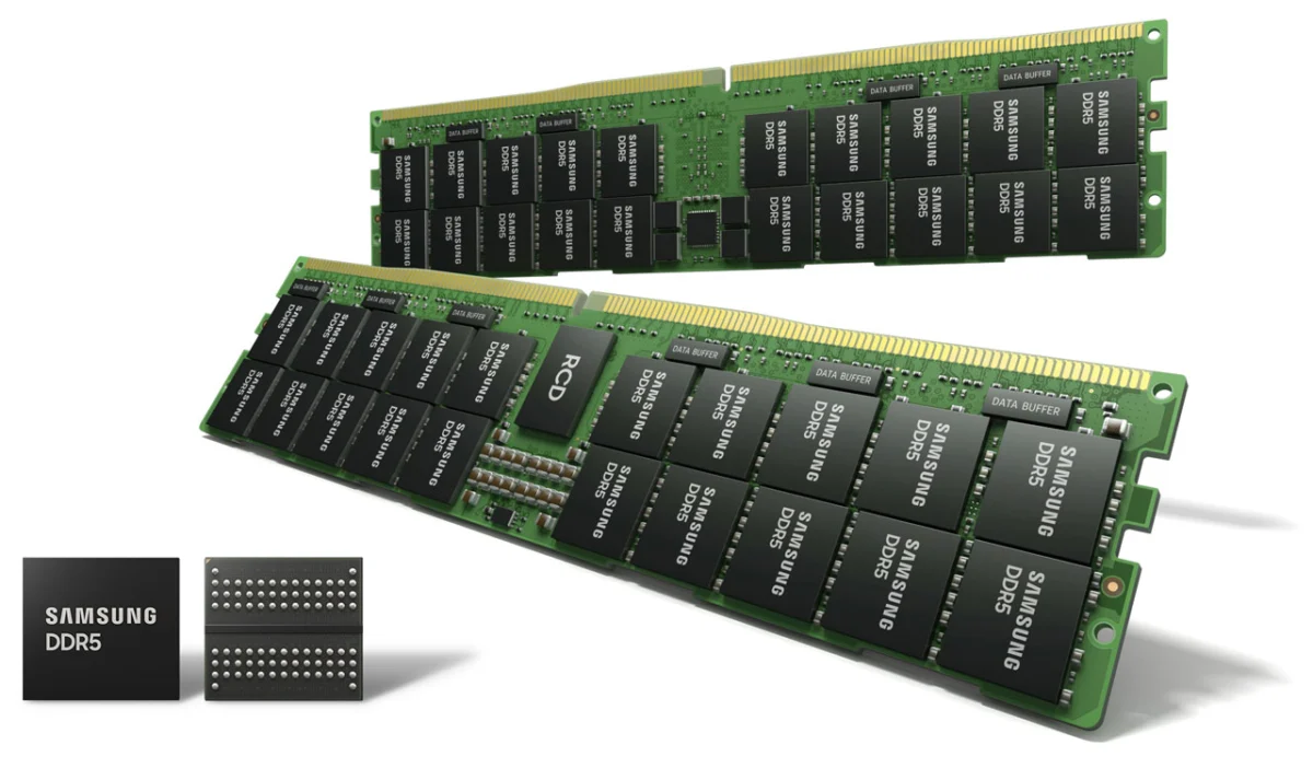
In a landmark development for the semiconductor industry, Samsung Electronics has officially commenced mass production of the world’s most advanced 14-nanometer (nm) Extreme Ultraviolet (EUV) DDR5 DRAM. This milestone not only cements Samsung’s leadership in high-density memory manufacturing but also signals a seismic shift in how computing platforms will handle the burgeoning demands of the AI, 5G, and metaverse-driven digital economy. By integrating five-layer EUV technology into its most refined process node to date, Samsung is effectively rewriting the rules of performance, efficiency, and capacity for the next generation of computing.
The Chronology of Innovation: From EUV Debut to Mass Production
Samsung’s journey toward the current 14nm breakthrough is a testament to the company’s aggressive investment in advanced lithography. The path began in earnest in 2020, when Samsung became the first memory manufacturer in the industry to successfully ship EUV-based DRAM. This initial foray served as the proving ground for the transition from traditional photolithography to EUV, a process essential for patterning the increasingly microscopic features required for sub-10nm class nodes.
Following that initial success, the company spent the intervening months refining its lithographic processes to overcome the yield and scalability challenges inherent in extreme miniaturization. By early 2021, reports from within the supply chain indicated that Samsung had reached a high level of maturity in its EUV processes, allowing for the stable production of its 14nm-class DRAM. The transition from the "first-gen" EUV approach to this five-layer EUV architecture represents a significant evolution, as it allows for far greater precision in the placement of circuits, effectively minimizing the interference that typically plagues high-density memory arrays.
Today, the industry is witnessing the direct result of this multi-year R&D cycle: a product that combines the absolute density of 14nm lithography with the precision of EUV, marking the most significant leap in memory fabrication since the introduction of 3D NAND.
Technical Specifications and Performance Metrics
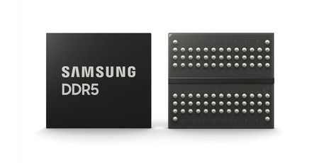
The core advantage of Samsung’s latest DDR5 offering lies in its unprecedented density and speed. By utilizing five layers of EUV, Samsung has managed to create the densest DRAM chips ever produced. This is not merely an incremental improvement; it is a fundamental shift in how bits are packed onto a silicon die.
Performance Gains
According to internal testing conducted by Samsung, the new 14nm DDR5 DRAM modules offer a 20 percent boost in overall productivity compared to the previous generation of DRAM. This performance gain is critical for modern computing environments where "data-driven" workflows—such as real-time AI training, massive database querying, and high-fidelity metaverse rendering—are becoming the standard rather than the exception.
Speed and Bandwidth
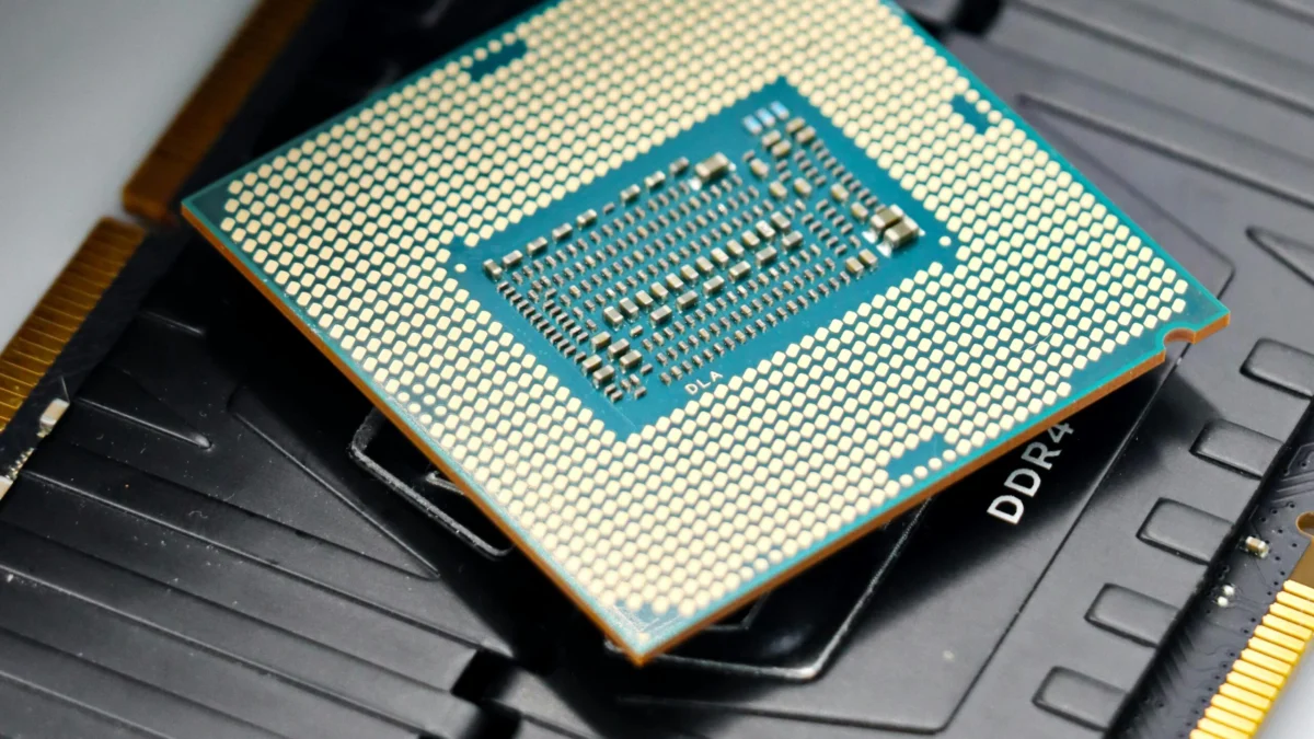
Perhaps the most immediately tangible benefit for the end-user is the jump in data transfer rates. While current DDR4 standards typically operate at around 3.2Gbps, Samsung’s new 14nm DDR5 modules are engineered to reach speeds of up to 7.2Gbps. This doubling of effective bandwidth provides the "breathing room" required by modern multi-core processors, such as Intel’s Alder Lake-S architecture, which require massive amounts of data throughput to keep their high-speed caches fed.
Efficiency Improvements
In addition to raw speed, the 14nm process offers significant gains in power efficiency, also hovering around the 20 percent mark. This efficiency is achieved by reducing the operating voltage and decreasing the power required for signal switching, a crucial development for both data centers looking to minimize their power footprint and mobile devices aiming to extend battery life during intensive tasks.
Official Responses and Industry Vision
The announcement was accompanied by a statement from Jooyoung Lee, Senior Vice President and Head of the DRAM Product & Technology team at Samsung Electronics. Lee framed the development as a critical milestone for the future of digital infrastructure.
"The application of our 14nm EUV technology represents a defining moment in the history of DRAM," Lee stated. "As we look toward a future dominated by the metaverse and artificial intelligence, the demand for memory that can handle massive throughput with extreme efficiency has never been greater. We are not just building faster memory; we are building the foundation upon which the next decade of computing innovation will be constructed."
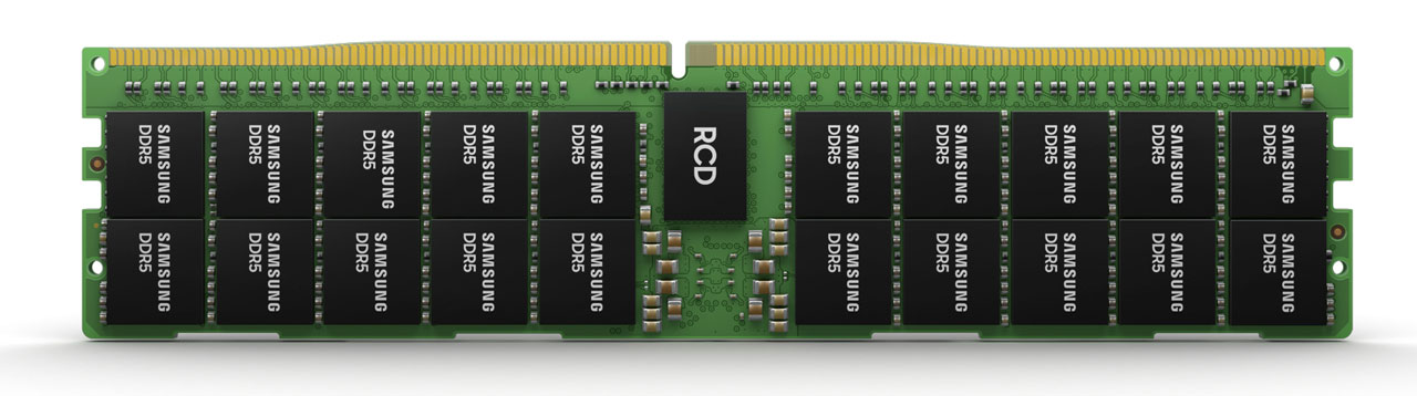
Samsung’s vision for this technology is clear: they intend to scale the 14nm process to support individual IC densities of up to 24Gb. If successfully realized, this would allow for the creation of massive 768GB DDR5 DIMMs. While the industry will likely see a phased rollout—starting with standard 64GB-per-stick configurations—the roadmap to higher-capacity modules ensures that enterprise-grade servers will soon have access to a level of memory density that was previously confined to specialized, multi-slot configurations.
Market Implications: The Transition to DDR5
The arrival of 14nm DDR5 is not without its market friction. As with any major architectural transition, there is a "crossover period" that presents challenges for consumers and manufacturers alike.
The Motherboard Conundrum
Hardware manufacturers are preparing for a bifurcated market. Leading motherboard vendors, such as Asus, have been spotted registering various versions of their upcoming Z690 series, with specific "D4" suffixes denoting support for the legacy DDR4 standard. This strategy is a clear concession to the expected high cost of DDR5 memory at launch. By offering motherboards that support both new and old standards, companies are ensuring that enthusiasts can upgrade their CPUs to the latest generation without being forced to pay the "early adopter tax" on memory.
The Pricing Premium
The concern over the cost of DDR5 is well-founded. Recent data from online retailers like Newegg suggests that the premium for early DDR5 kits will be substantial. For instance, a GeIL Polaris RGB SYNC 32GB (2 x 16GB) DDR5-4800 kit was recently spotted with a price tag of US$349.99. In international markets, the pricing reflects a similar trend, with Japanese listings hovering around JPY45,174.
These figures translate to approximately £250 to £300, a significant markup over high-performance DDR4 kits that currently offer similar capacities for a fraction of the price. While these prices are expected to stabilize as production ramps up and the 14nm process yields improve, early adopters should be prepared for a substantial initial investment.
Long-term Outlook: A New Standard for Computing
Samsung’s achievement is a clear signal that the semiconductor industry is successfully navigating the "end of Moore’s Law" by shifting focus toward innovative lithography and packaging techniques. By mastering EUV at the 14nm node, Samsung has not only extended the life of traditional DRAM architectures but has also created a roadmap for future scaling.
The implications for the broader tech ecosystem are profound. As AI models become more complex and the metaverse demands greater graphical and processing fidelity, the bottleneck in computing is increasingly shifting toward memory bandwidth and capacity. By addressing these constraints today, Samsung is ensuring that the hardware of tomorrow can keep pace with the software innovations that are currently being developed.
Furthermore, the focus on 24Gb IC density suggests that Samsung is looking far beyond the desktop PC market. The goal is to reshape the server and cloud-computing landscape, where power-to-performance ratios are the primary drivers of capital expenditure. As the industry moves toward 768GB DIMMs, the traditional limitations of data center memory capacity will be effectively dismantled, allowing for unprecedented scalability in cloud-native applications.
In conclusion, while the average consumer might experience a period of sticker shock as DDR5 hits the retail shelves, the long-term trajectory is one of progress. Samsung’s 14nm EUV DDR5 DRAM is more than just a component; it is the enabler of a new era of high-performance computing. Whether in the data center, the AI-driven research lab, or the enthusiast’s gaming rig, this technological leap promises to deliver the speed and efficiency required to power the digital demands of the next decade. As we stand on the precipice of this transition, it is clear that the future of memory is not just smaller—it is faster, denser, and fundamentally more capable.