
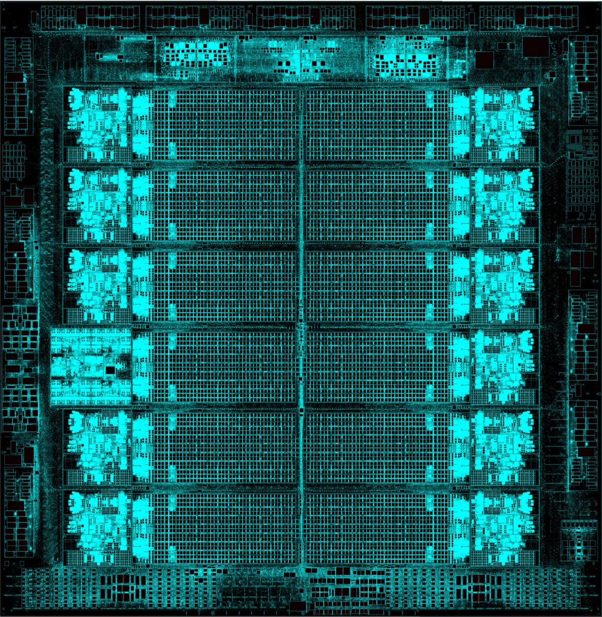
In a move that promises to reshape the landscape of enterprise computing, IBM has unveiled its next-generation processor architecture at the Hot Chips 2026 conference. This groundbreaking silicon marks a departure from traditional mainframe design, as it becomes the first in the industry to natively support dual Instruction Set Architecture (ISA) execution within a single core. By integrating z/Architecture and AArch64 (Arm) capabilities into one cohesive unit, IBM is effectively bridging the gap between legacy mission-critical stability and the vast, modern software ecosystem of the Arm architecture.
Main Facts: A Dual-ISA Milestone
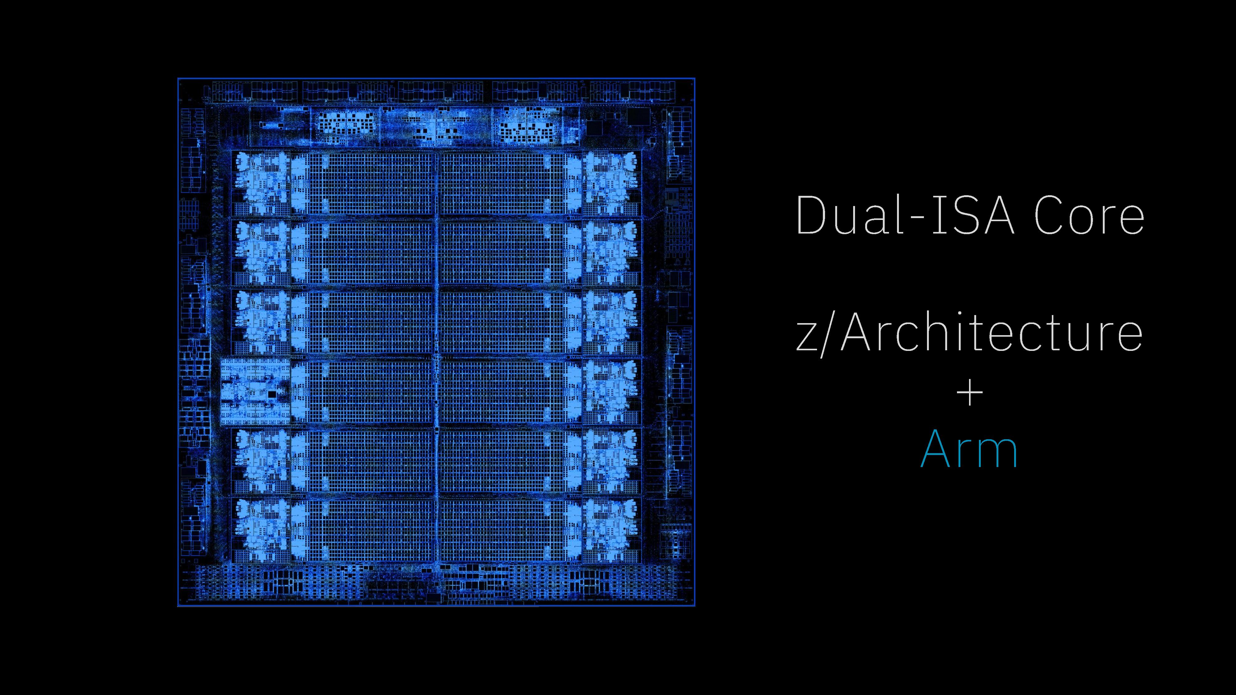
The core innovation behind IBM’s latest silicon is the transition from a monolithic ISA to a flexible, dual-ISA design. Unlike heterogeneous systems that pack separate Arm and proprietary cores onto a single die, IBM has engineered a "true" dual-ISA core. This allows the processor to switch between z/Architecture—the foundation of IBM’s legendary mainframes—and the Arm AArch64 instruction set dynamically.
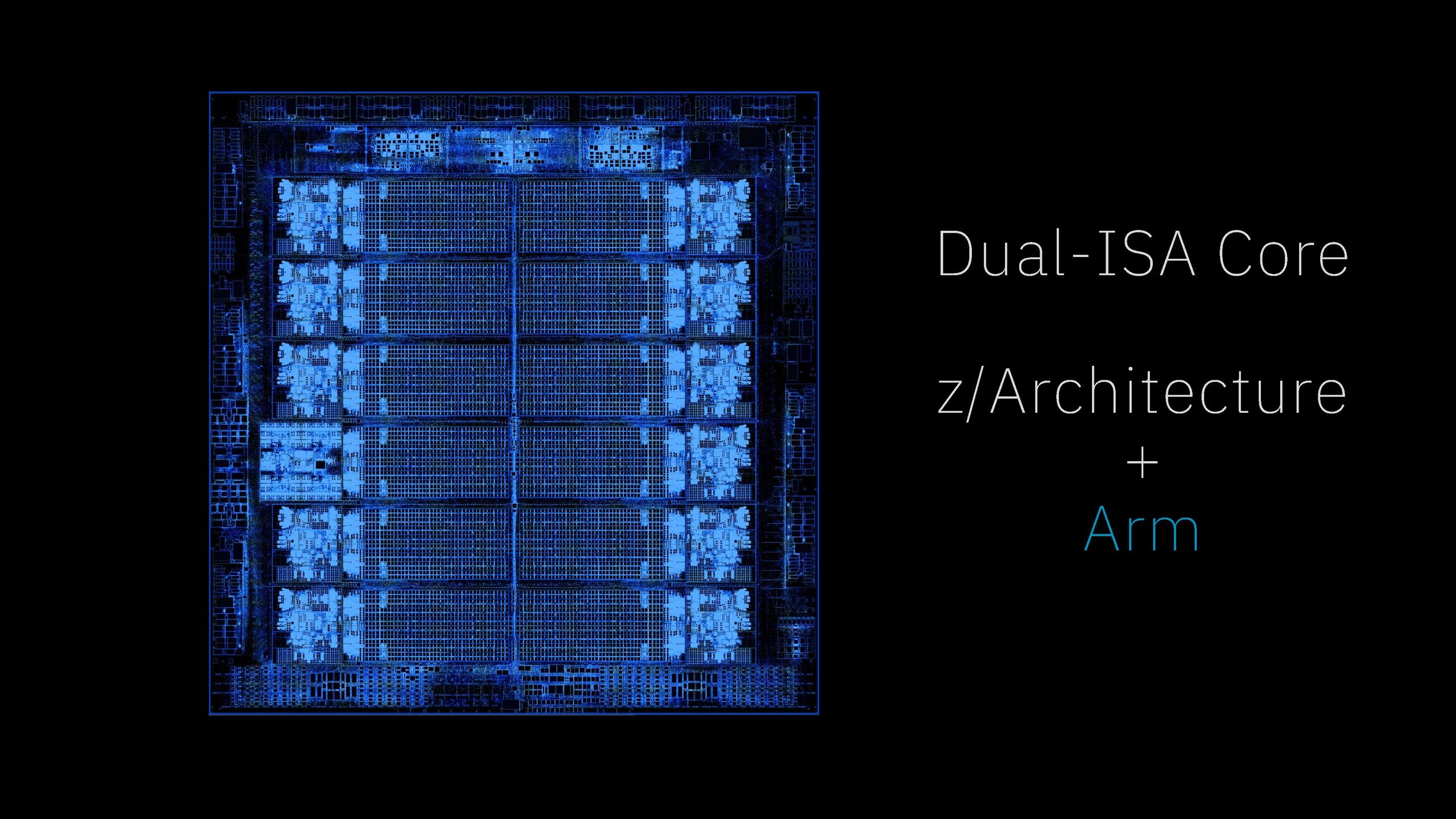
According to IBM’s technical disclosures, this switching happens at the nanosecond level. The processor is designed to treat both ISAs as "first-class citizens," ensuring that neither architecture is treated as a secondary emulation or virtualized afterthought. This design philosophy is aimed at allowing businesses to consolidate their infrastructure, eliminating the need to maintain separate x86/Arm server farms alongside IBM Z mainframes. By bringing Arm-based workloads directly into the mainframe environment, IBM is positioning its hardware as a unified engine for both traditional transaction processing and modern, containerized AI development.
The Chronology: From Collaboration to Silicon
The roots of this technological leap trace back to a strategic collaboration between IBM and Arm, which was publicly announced in April. For years, the mainframe industry faced a persistent challenge: while IBM Z remained the backbone of the world’s most critical financial and governmental data systems, it was increasingly isolated from the rapid innovation occurring in the Arm ecosystem.
Developers working on AI, cloud-native applications, and modern middleware were overwhelmingly targeting x86 or Arm architectures. Consequently, porting software to the IBM s390x environment became a bottleneck for enterprise agility. By teaming up with Arm, IBM sought to address this friction at the silicon level rather than relying on software emulation or porting services, which often proved unsustainable in the long run.
Following the initial announcement, the development cycle accelerated rapidly. By the time of the Hot Chips 2026 presentation, IBM was able to demonstrate not just a concept, but a production-ready design that pushes the boundaries of current fabrication. The integration of Arm v9.3, complete with Scalable Vector Extension (SVE) support, represents the culmination of this partnership, effectively allowing the mainframe to act as a native host for the global Arm software library.
Supporting Data and Technical Specifications
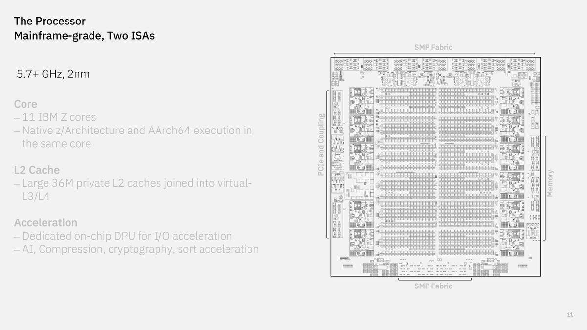
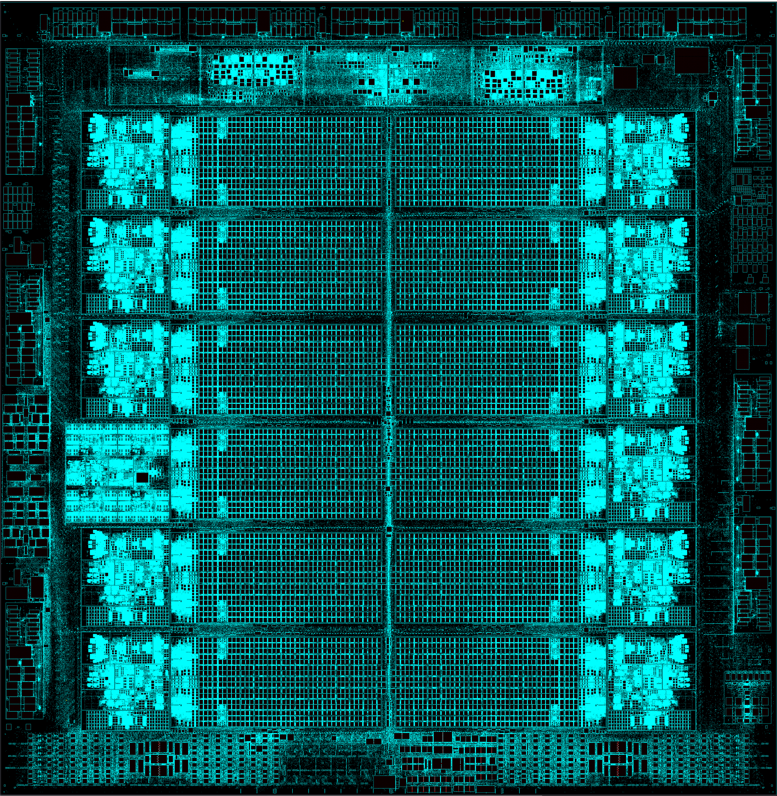
The sheer engineering effort required to make this work is reflected in the technical specifications of the new processor. The chip is manufactured on an advanced 2nm process node and features 11 high-performance cores per processor, each capable of a base clock frequency of 5.7 GHz.
To contextualize this progress, one must look at its predecessor, the Telum II processor introduced in 2024. The Telum II was a powerhouse in its own right, with eight cores running at 5.5 GHz. The new dual-ISA chip not only increases core counts and clock speeds but also significantly enhances the memory hierarchy. The chip features 36 MB of private L2 cache per core, alongside a staggering 432 MB of virtual L3 cache and a massive 3.5 GB of virtual L4 cache.
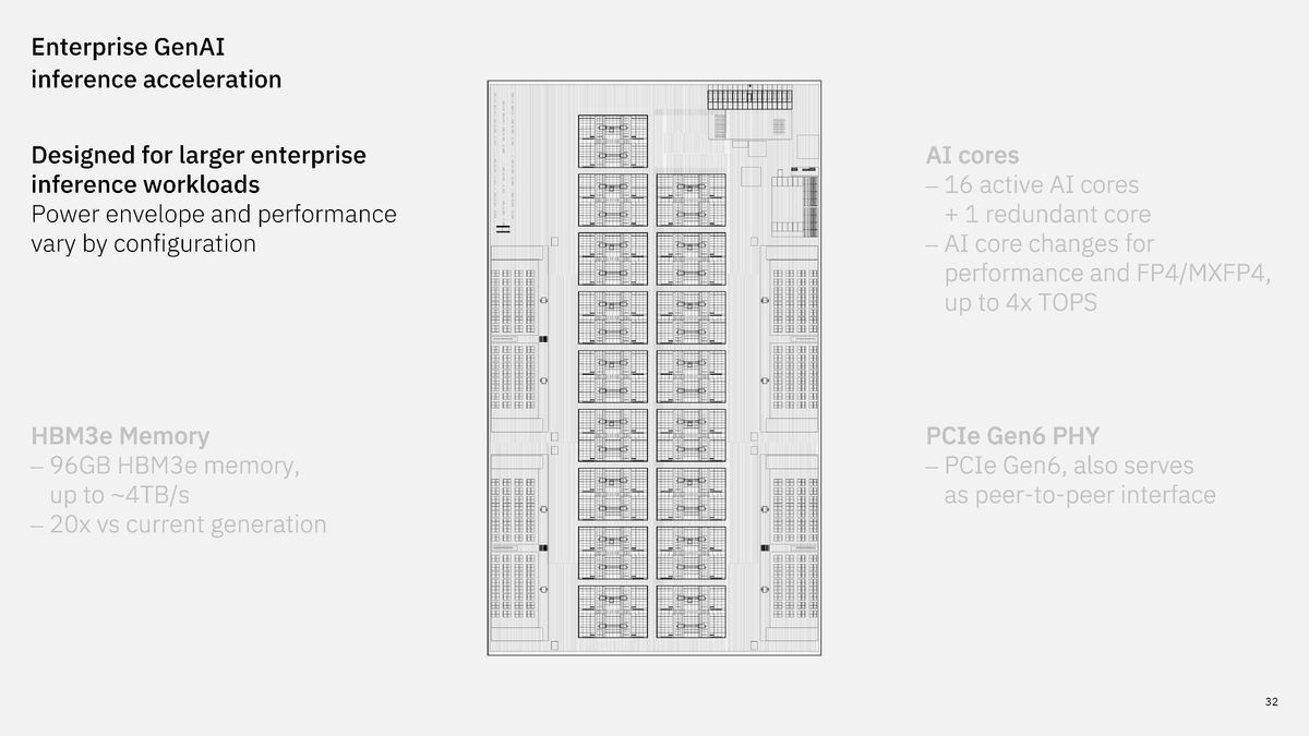
The architecture also retains and upgrades the on-chip Data Processing Unit (DPU) and hardware accelerators for AI, compression, and cryptography—functions that have become synonymous with IBM’s security-first approach. Furthermore, the accompanying next-gen Spyre AI accelerator has received a significant overhaul. Shifting from LPDDR5 to HBM3e (High Bandwidth Memory), the new accelerator provides 96 GB of memory per unit, delivering 4TB/s of bandwidth—a 20-fold increase over the previous generation’s memory subsystem. This is specifically optimized for newer AI data formats, such as FP4 and MXFP4, ensuring that the mainframe remains relevant in the age of large-scale generative AI.
Official Responses and Strategic Vision
IBM leadership has been vocal about the necessity of this pivot. Tina Tarquinio, Chief Product Officer for IBM Z and LinuxONE, emphasized that the company’s traditional approach to porting software was reaching a point of diminishing returns.
"We would never be able to work with all of them," Tarquinio stated, referring to the thousands of software projects migrating toward Arm. The strategic vision here is to allow Arm-based virtual machines to run with native-level performance. Because the core is fundamentally an Arm-capable device at the hardware level, the performance penalty associated with traditional virtualization is largely mitigated.
IBM maintains that its core mission—reliability—remains untouched. The system is designed to provide "six-nines" (99.999999%) of uptime, which IBM calculates as roughly 0.032 seconds of downtime per year. By integrating Arm support into this ultra-reliable architecture, IBM hopes to convince enterprise clients that they no longer need to sacrifice the uptime of a mainframe to gain the software versatility of a commodity Arm server.
Architectural Deep Dive: How the "Dual" Works
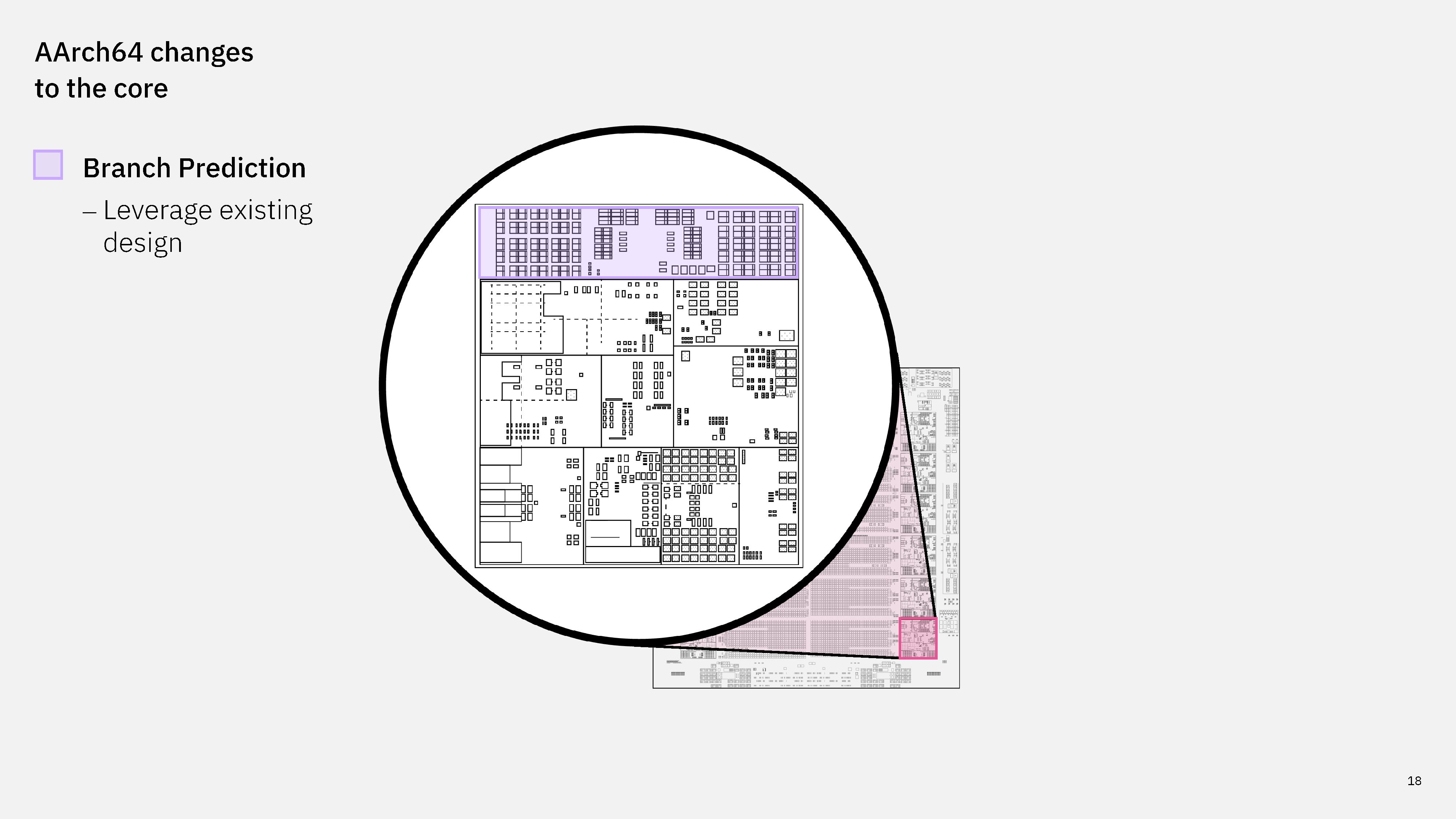
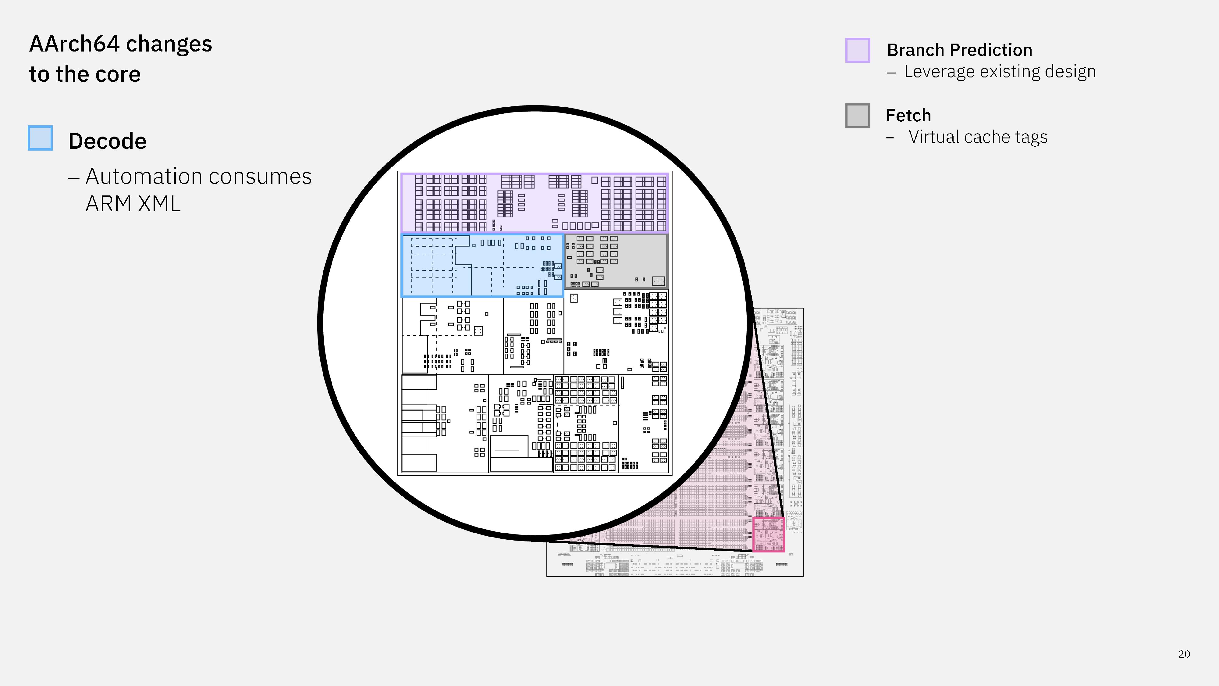
The "magic" of the dual-ISA core lies in its granular execution. IBM’s engineers utilized automation tools to parse the Arm XML specifications, allowing the chip’s internal logic to decode AArch64 instructions natively.
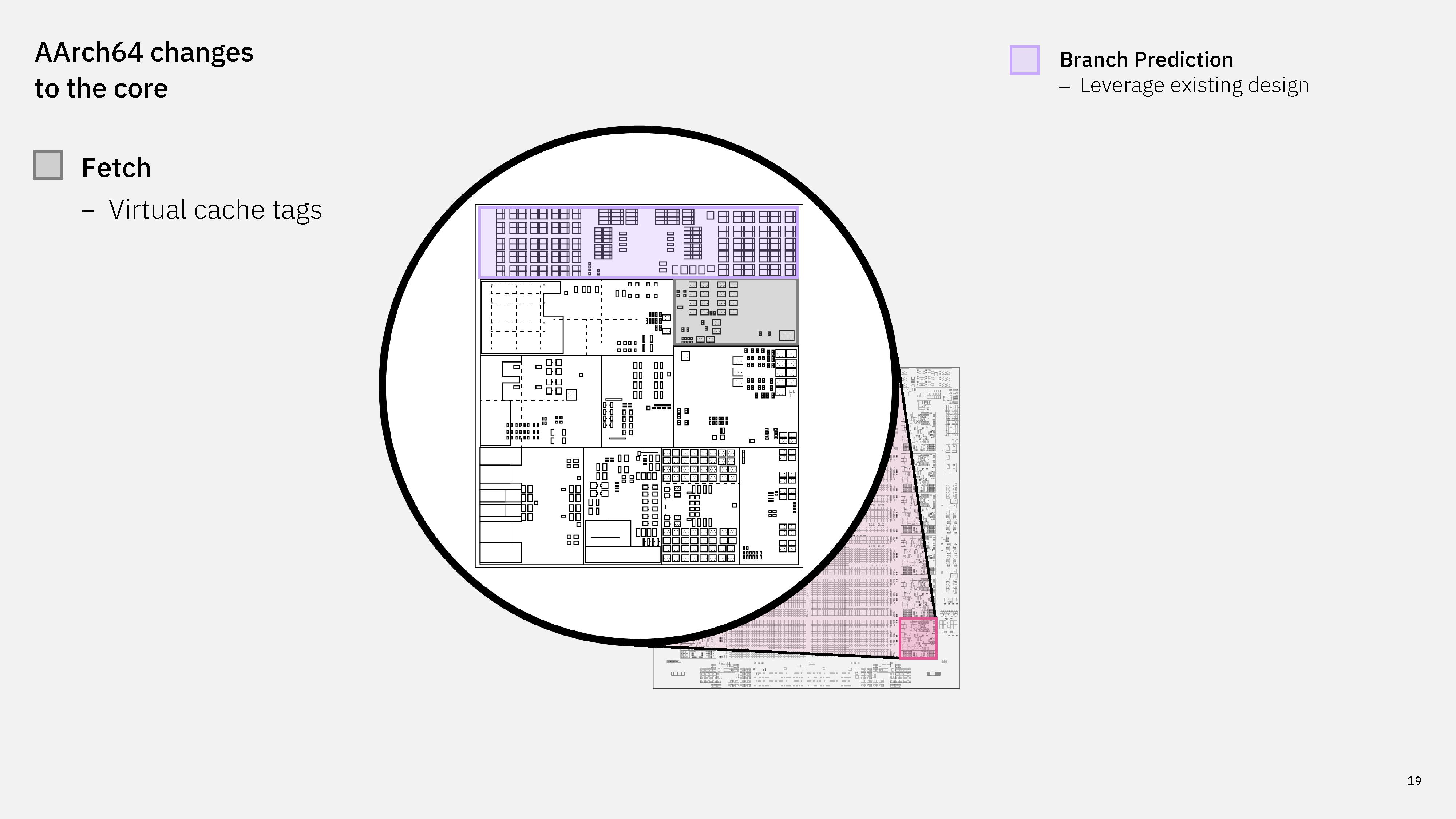
- Fetch Engine: IBM leverages virtual cache tags to allow for rapid data retrieval without the overhead typically associated with instruction translation.
- Decode Engine: This represents the largest area of silicon expansion. By implementing a full hardware decoder for 2,792 AArch64 instructions, the chip can process Arm code without requiring an intermediate translation layer.
- Dispatch: The design team repurposed general-purpose register renaming for the banked general registers (16 through 31), allowing the processor to toggle between register states when switching architectures.
- Arithmetic and Load/Store Units: As IBM noted, "addition is addition." The data flow for basic math and memory operations is shared between the two ISAs, drastically reducing the physical footprint of the core. However, dedicated hardware structures were added for SVE and floating-point types like FP16 to satisfy the requirements of the Arm specification.
- Translation Engine: The Translation Lookaside Buffer (TLB) is shared, but the system employs a new page-walk mechanism to handle the specific memory mapping requirements of the AArch64 instruction set.
Implications for the Future of Enterprise IT
The implications of this development are profound. For decades, the IT world has been divided into "silos": the mainframe for transaction-heavy, high-security tasks, and the x86/Arm cloud for everything else. By breaking down the ISA barrier, IBM is signaling the end of this strict segregation.
1. Data Gravity and AI
Mainframes are the vaults of the global economy. By allowing AI models trained on Arm-based cloud infrastructure to run directly on the mainframe, IBM is enabling "AI at the point of data." This eliminates the need to move sensitive financial or personal data across a network to an AI server, drastically improving both latency and security.
2. Software Consolidation
For enterprise CTOs, the ability to run Arm software natively on a mainframe means a reduced footprint in the data center. It lowers power consumption, simplifies the management stack, and reduces the number of disparate platforms that need to be patched and secured.
3. The Future of the Mainframe Roadmap
IBM typically refreshes its mainframe lineup every 2.5 to 3 years. Given that the z17 was revealed in 2024, the industry can expect the dual-ISA processor to debut in the upcoming z18 series. As with all mainframe transitions, the rollout will be measured and institutional, but the underlying technology is now ready.
In conclusion, IBM’s decision to build a dual-ISA processor is a defensive yet visionary move. It acknowledges that while the mainframe is irreplaceable, it cannot remain a closed garden. By embracing the Arm ecosystem, IBM has not only future-proofed its most important hardware line but has also provided a blueprint for how legacy and modern computing can coexist within the same silicon heart. The result is a machine that is as versatile as it is reliable—a combination that, in the world of high-stakes enterprise computing, is invaluable.