
Nvidia CEO Jensen Huang has publicly addressed and dismissed recent reports suggesting that the company’s highly anticipated next-generation AI platform, Vera Rubin, is facing significant development hurdles. Speaking on the sidelines of an industry event in Japan, Huang sought to project confidence, assuring investors and partners that the platform is not only on track but currently entering a massive production phase.
However, while Huang’s firm rebuttal serves to stabilize market sentiment regarding the core Rubin architecture, the technology landscape remains complex. Industry analysts continue to scrutinize the nuances of Nvidia’s hardware rollout, particularly regarding the high-end rack-scale systems that define the future of AI supercomputing.
The State of the Rubin Platform: A Direct Rebuttal
The primary source of concern for many stakeholders was a wave of rumors suggesting that the Rubin family of products—Nvidia’s answer to the evolving demands of large-scale generative AI training—was suffering from delays.
"The reports about Vera Rubin delays are not true," Huang stated, as reported by Bloomberg. "Vera Rubin is already in production. Giant amounts of production are incoming."
This statement is intended to signal to the market that the foundation of Nvidia’s next revenue engine is secure. Since the official confirmation of the Rubin platform’s production in January and the subsequent sampling phase in February, Nvidia has been under pressure to prove that its aggressive roadmap can keep pace with the exponential growth of AI infrastructure. By emphasizing "giant" volumes, Huang is essentially telling shareholders that the supply chain is primed to meet the insatiable demand for the upcoming Vera CPUs and Rubin GPUs.
Chronology: From Concept to Production
To understand the current tension, one must look at the timeline of Nvidia’s recent hardware trajectory:

- January 2026: Nvidia officially confirms that the Vera Rubin platform is entering production, marking a critical milestone in the transition from the Hopper and Blackwell architectures.
- February 2026: The company begins the critical sampling phase, delivering early units to lead customers to facilitate software optimization and system-level validation.
- Mid-2026: Reports surface regarding potential manufacturing challenges, specifically concerning the high-density, copper-interconnect-heavy "Kyber" rack-scale systems.
- July 2026: Jensen Huang addresses the market, explicitly denying widespread delays for the Rubin platform and reaffirming the company’s production readiness.
Despite this clear progression, the conversation has shifted toward the specific implementation challenges of the "Ultra" variants and the ambitious rack-scale solutions that follow.
Decoding the "Kyber" and "Rubin Ultra" Challenges
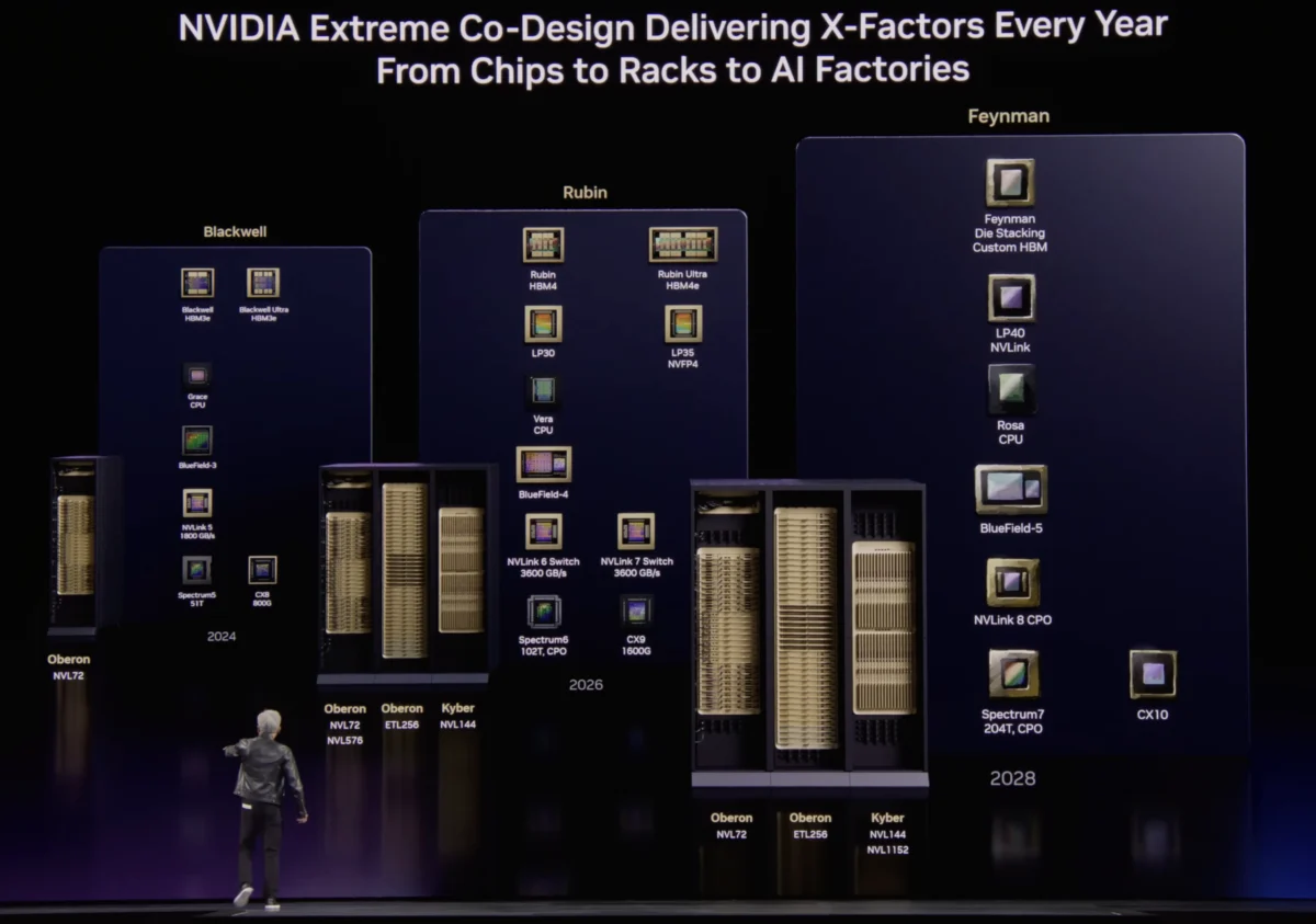
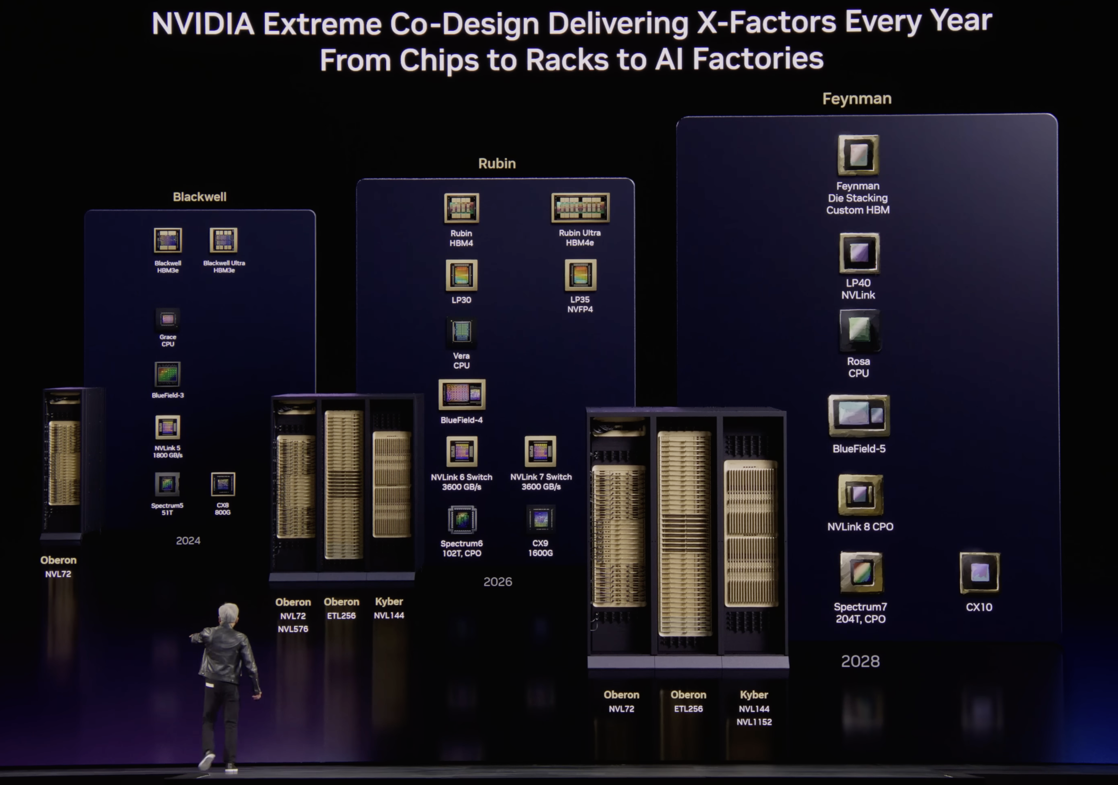
While the base Rubin platform appears to be moving forward smoothly, the technical hurdles associated with the "Kyber" NVL144 rack-scale solution remain a focal point of industry analysis.
The Kyber architecture was designed to be a behemoth, capable of connecting 144 Rubin Ultra GPUs using a sophisticated, copper-based NVLink 7 scale-up fabric. The technical challenge, according to industry reports, lies not in the silicon itself—the GPUs are reportedly sound—but in the physical infrastructure: the massive, complex PCB (printed circuit board) midplane required to carry high-speed electrical signals between such a high number of interconnected components.
The reported delay of the Kyber NVL144 from 2027 to 2028 suggests that the engineering requirements for such dense copper interconnects are pushing the boundaries of current manufacturing capabilities. Furthermore, the rumored cancellation of an alternative "dual-rack" design, which would have back-to-back mounted "Oberon" racks to expand the NVLink domain, indicates that Nvidia is being highly selective about which engineering compromises it is willing to offer its customers.
The CPO Conundrum: Optical Interconnects as the Future
The conversation surrounding these delays inevitably leads to the topic of Co-Packaged Optics (CPO). Nvidia’s planned NVL576 rack-scale solution was originally intended to utilize CPO technology to bridge the communication gap between NVSwitches.
The postponement of this system—or its limitation to very small, specialized quantities—highlights the "ongoing CPO challenges" that have hampered the industry at large. CPO, while theoretically superior to copper in terms of signal integrity and energy efficiency at high speeds, is notoriously difficult to manufacture at scale.

There is an open question as to whether the optical technology intended for the NVL576 could be adapted to solve the connectivity issues seen in the Kyber design. While theoretically possible, it is unclear if the bandwidth and latency characteristics of such an implementation would meet the stringent requirements of a 144-GPU domain.
Competitive Implications: The 2027-2028 Window
The uncertainty surrounding the availability of 144-way scale-up systems for the Rubin generation creates a potential opening for competitors. If Nvidia is limited to 72-way scale-up systems until 2028, the competitive landscape for high-end AI training clusters will shift significantly.
AMD’s Growing Ambition
AMD is currently positioning its "Mega Pod" architecture—utilizing Verano CPUs and Instinct MI500-series accelerators—as a viable alternative. With a capacity of up to 256 accelerators per cluster, AMD’s roadmap suggests a level of scalability that could challenge Nvidia’s dominance in the ultra-large-scale cluster market by 2027.
The Google Factor
Google remains a unique player in the space. Its TPU (Tensor Processing Unit) strategy has evolved to provide massive scale-up domains, with the TPU 8i and 8t variants offering extreme density. With the ability to pack thousands of chips into a single low-latency domain, Google’s internal infrastructure continues to be a benchmark for what is possible outside of the traditional GPU-based merchant market.
Official Responses and Strategic Positioning
When pressed by Tom’s Hardware regarding the roadmap status, an Nvidia spokesperson provided a characteristically concise response: "Our roadmap is intact."
This statement serves as the company’s official line, intended to prevent the erosion of market confidence. It neither confirms nor denies the specific reports regarding manufacturing setbacks for the Kyber rack or the Rubin Ultra chiplet configuration. Instead, it underscores a strategic pivot: focusing on what is being produced—the "giant" quantities of Rubin—rather than the specific timelines of the most complex, niche rack configurations.
Conclusion: The Road Ahead
Nvidia is currently navigating the transition from a hardware supplier to an infrastructure provider. The complexity of the Rubin generation, characterized by a move toward denser interconnections and, eventually, co-packaged optics, represents the next frontier of high-performance computing.
While Jensen Huang’s recent comments should reassure the market that the core Rubin platform is ready for mass deployment, the challenges associated with the Kyber NVL144 and the broader shift to optical interconnects remain significant. The next 18 to 24 months will be a defining period for Nvidia. Whether the company can maintain its lead depends not just on the performance of its GPUs, but on its ability to master the physical, mechanical, and optical challenges of building the world’s most powerful AI supercomputers.
As the industry looks toward 2027 and 2028, the race for massive-scale connectivity will be the ultimate test of Nvidia’s engineering prowess against the rising capabilities of competitors like AMD and the custom silicon efforts of the hyperscalers. For now, the "giant" production of Rubin remains the company’s strongest defense.