
In a move that signals a deeper strategic integration into the foundation of custom artificial intelligence silicon, Nvidia has announced the launch of NVHBM. This custom-engineered high-bandwidth memory (HBM) base die represents a significant expansion of Nvidia’s NVLink Fusion program. By providing partners with the specific building blocks required to interface custom processors with the NVLink scale-up domain, Nvidia is effectively standardizing the architecture that will power the next generation of massive, rack-scale AI accelerators.
This development does not merely replace current memory standards; rather, it introduces a highly optimized, custom-validated framework designed to alleviate the most critical bottlenecks in contemporary AI infrastructure: bandwidth, power consumption, and physical space constraints on the silicon die.
The Core Innovation: What is NVHBM?
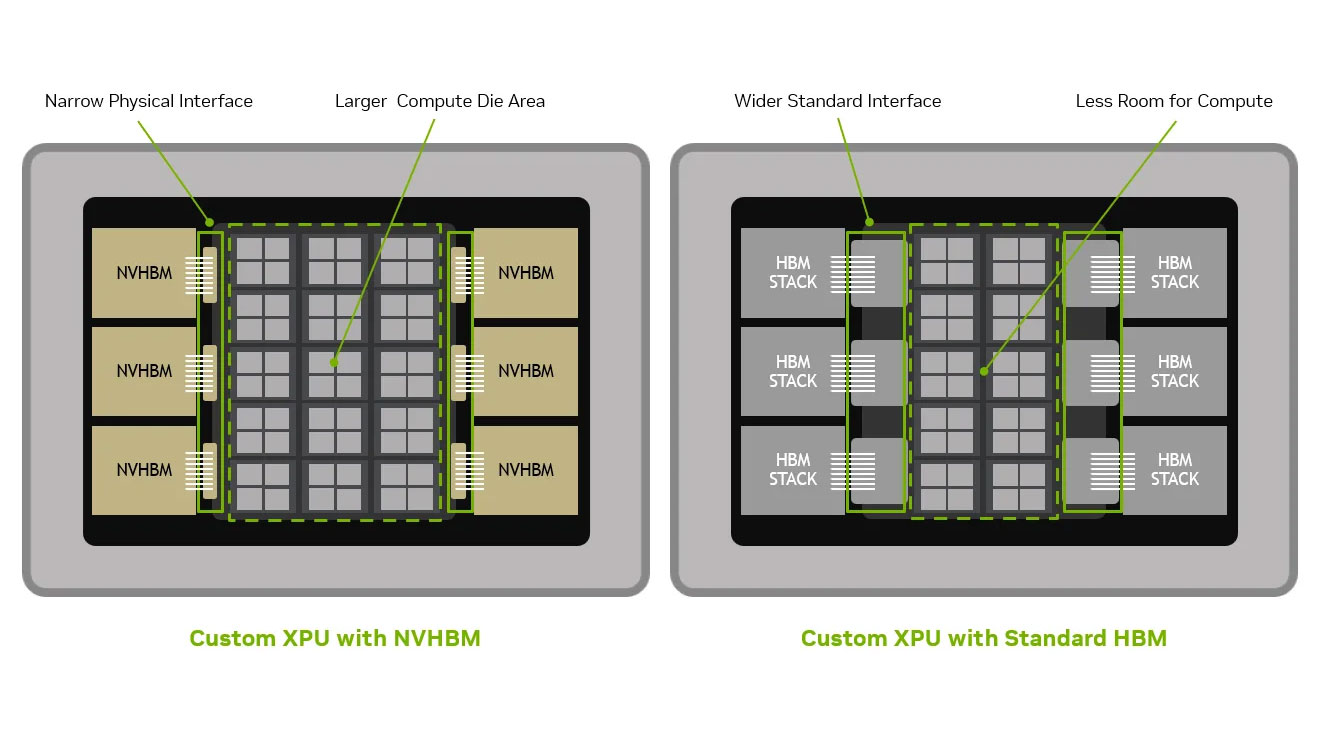
To understand the significance of NVHBM, one must first look at the traditional constraints of AI chip design. Modern AI accelerators rely on High Bandwidth Memory (HBM) to feed massive datasets—model weights and KV caches—to the processing units at speeds that commodity DRAM cannot achieve. In conventional designs, the HBM controller is typically embedded directly onto the primary silicon die (the GPU or AI accelerator). This consumes valuable, expensive real estate on the chip, complicates the layout of the interposer, and contributes to the thermal and power density challenges that designers fight at every turn.
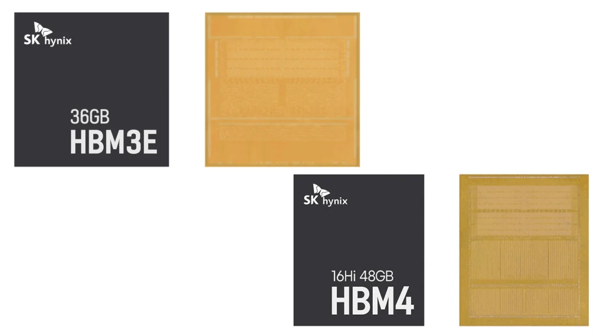
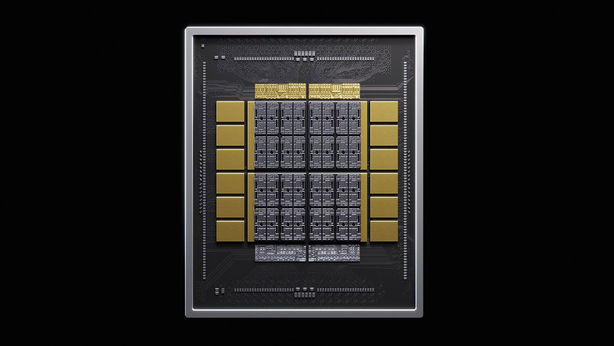
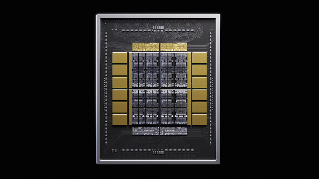
Nvidia’s NVHBM changes this architecture by migrating the memory controller from the main compute die into the base die of the HBM stack itself. By integrating a custom PHY (physical interface) into this base die, Nvidia provides a streamlined, pre-validated solution for its partners. This allows designers to bypass the arduous process of implementing an HBM controller from the ground up, significantly accelerating the time-to-market for custom-silicon ventures.
Chronology: From Blackwell to the Future of Custom Silicon
The trajectory of Nvidia’s infrastructure strategy has been one of increasing vertical integration. The journey to NVHBM can be traced through the following key developments:
- The Rise of NVLink: Originally a specialized interconnect for Nvidia’s own GPUs, NVLink evolved into a foundational technology for data center-scale compute, enabling multiple processors to act as a single, coherent system.
- The Vera Rubin Era: The announcement of the Vera Rubin NVL72 rack-scale accelerator showcased Nvidia’s ambition to dominate not just the chip, but the entire rack environment. The focus shifted toward minimizing "wasted" energy during data movement.
- The NVLink Fusion Program: Recognizing the demand from hyperscalers (like Amazon, Microsoft, and Google) to build their own custom silicon, Nvidia opened up its "scale-up domain." This allowed partners to marry their custom compute logic with Nvidia’s high-speed networking fabric.
- The Launch of NVHBM: Today’s announcement serves as the natural evolution of the Fusion program. By standardizing the memory interface, Nvidia is creating an ecosystem where custom chips can plug directly into the high-speed memory and networking fabric that Nvidia has perfected.
Supporting Data: Efficiency and Throughput Metrics
Nvidia’s technical white papers and disclosures surrounding the NVHBM launch emphasize three primary performance gains. These figures are critical for hyperscalers operating in an environment where "tokens per second" is the ultimate currency.
1. 30% Higher Bandwidth per Stack
Standard HBM4e is already a marvel of engineering, but NVHBM pushes the boundaries further. By optimizing the base die architecture, the solution provides up to 30% higher bandwidth per stack. In memory-bandwidth-bound AI workloads, this allows for significantly faster token generation rates during inference, effectively lowering the latency for large language models (LLMs).
2. 30% More Compute Real Estate
The migration of the memory controller from the main die to the HBM base die is perhaps the most impactful architectural change. By removing this complex circuitry from the primary chip, developers can reallocate that "precious real estate" to increase compute density. This translates to 30% more space for logic, floating-point units, and other specialized accelerators, allowing for more powerful chips without increasing the overall package size.
3. 15% Power Efficiency Gains
Energy efficiency is the primary constraint in the modern data center. Nvidia’s internal metrics suggest that NVHBM consumes 15% less power than commodity HBM4e. In a rack-scale system consisting of thousands of interconnected chips, these savings compound exponentially. This power surplus can be "banked" to improve performance-per-watt metrics or reallocated to allow for higher clock speeds within the same TDP (Thermal Design Power) envelope.
Official Responses and Strategic Partnerships
The impact of NVHBM is best reflected in the response from industry leaders. Amazon’s Annapurna Labs has been confirmed as the inaugural partner for this technology.
"We look forward to this technology collaboration to benefit future AWS infrastructure designs," stated Nafea Bshara, Vice President of Annapurna Labs.
This partnership is particularly telling. Annapurna’s Trainium 4 AI chips already leverage the NVLink Fusion scale-up interface. By adopting NVHBM, AWS is signaling a shift toward a future where their custom infrastructure is built on a "Nvidia-certified" foundation of high-speed interconnects and memory, effectively creating a hybrid ecosystem that combines the efficiency of custom silicon with the reliability and speed of Nvidia’s proprietary standards.
Implications for the AI Hardware Landscape
The introduction of NVHBM carries profound implications for the semiconductor industry:
The Consolidation of the "Custom Silicon" Market
Nvidia is essentially creating a "walled garden" that is nonetheless open to its most powerful partners. By standardizing the memory and interconnect layer, Nvidia makes it easier for companies to build their own chips, but it ensures those chips are optimized for Nvidia’s ecosystem. This reduces the friction for partners to switch to Nvidia-integrated platforms, reinforcing the company’s dominance in the AI infrastructure market.
A New Standard for Interposer Routing
Advanced packaging—the art of connecting multiple dies (chiplets) onto a single substrate—is becoming the defining challenge of the 2020s. NVHBM simplifies interposer routing, the "wiring" that connects the compute die to the memory stacks. By streamlining this, Nvidia is reducing the likelihood of yield issues and manufacturing complexity, which are major cost drivers in high-end chip production.
The "Wasted Watt" Doctrine
Nvidia’s persistent messaging regarding the "Vera Rubin" rollout centers on the philosophy that every watt not used for token production is a waste. NVHBM is the physical manifestation of this doctrine. By optimizing data movement, Nvidia is addressing the "memory wall"—the phenomenon where processors are so fast that they spend most of their time waiting for data. By shortening the path and increasing the speed of that data, NVHBM helps keep the silicon fed, maximizing the utility of every transistor.
Conclusion: A Strategic Pivot
It is important to note that NVHBM is not currently slated for the Rubin systems already in production; it is a forward-looking technology for future designs. However, its existence signals that the future of AI will not be defined by monolithic, off-the-shelf GPUs alone. Instead, the future belongs to highly customized, domain-specific silicon that sits atop a robust, standardized, and high-performance "plumbing" system—provided by Nvidia.
As we move toward the next generation of AI infrastructure, the battleground will not just be who has the most powerful core, but who has the most efficient memory and the most coherent interconnect. With NVHBM, Nvidia is ensuring that even if its partners decide to build their own compute engines, they will still be operating within the framework that Nvidia has meticulously architected.