

Nvidia is no longer content with merely being the primary supplier of AI accelerators for the world’s data centers. With the formalization of its "Spark" roadmap, the chip giant is signaling a permanent, long-term commitment to the consumer and professional Windows PC market. By fusing its high-performance graphics architectures with custom-designed ARM processors, Nvidia is aiming to redefine the performance expectations for desktop and mobile computing.
The debut of the "RTX Spark Superchip" is not merely a product launch; it is the culmination of years of development, internal pivots, and market anticipation. As the industry watches this new chapter unfold, the underlying message is clear: Nvidia intends to be as influential in the client PC space as it has become in the era of generative AI.
The Genesis of the Spark Ecosystem
The arrival of the first Spark-branded chip in the Windows ecosystem has been a long time coming. For industry observers, the technology is far from a surprise; it is a "known quantity" that has been teased through various iterations since CES 2025. Initially codenamed "Project Digits" and featuring the GB10 architecture, the chip faced a turbulent journey from the lab to the consumer shelf.
A Tortuous Road to Market
The GB10, now branded as the RTX Spark Superchip, was originally projected to make a splash during the Computex 2025 cycle. During that period, engineering samples were spotted in various notebook prototypes, fueling rumors of an imminent launch. However, the path to commercial availability was fraught with challenges. Reports of design flaws in the N1x series, coupled with the complexities of optimizing the Windows on ARM ecosystem, forced Nvidia to push back the rollout.
The chip eventually reached professional workstations during the winter of 2025, but its formal entry into the broader Windows PC market has only just been solidified. This delay highlights the high bar Nvidia set for itself: entering the PC market requires more than just raw silicon performance; it requires seamless integration with a legacy operating system environment that is currently undergoing its own tectonic shift toward ARM compatibility.
A Two-Year Rhythm: The New Roadmap
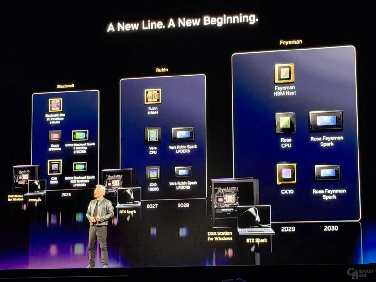
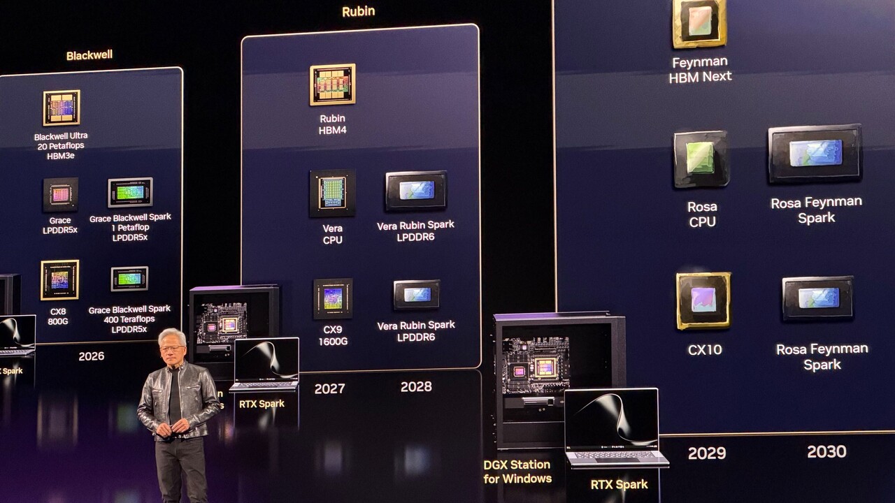
Perhaps the most significant revelation from Nvidia’s latest briefing is the establishment of a fixed two-year cadence for the Spark product line. This strategic "tick-tock" approach mirrors the company’s successful data center GPU cycles, providing OEMs and enterprise customers with a predictable window for hardware refreshes.
The Vera Rubin Spark (2028)
The first major successor to the current generation is scheduled for 2028: the Vera Rubin Spark. By the time this chip hits the market, the memory landscape will have matured significantly. Nvidia has confirmed that the Vera Rubin generation will take full advantage of the broader LPDDR6 ecosystem. This transition is critical, as memory bandwidth has historically been the primary bottleneck for high-performance ARM-based SoC designs. By aligning the Rubin launch with the maturation of LPDDR6, Nvidia aims to deliver a massive uplift in sustained compute performance.
The Rosa Feynman Era
Looking further ahead, Nvidia has outlined the architecture for the post-Rubin era. The Feynman GPU generation will be paired with the Rosa ARM CPU series. This combination, dubbed "Rosa Feynman," represents the next evolution of the Spark concept. While specific details regarding memory standards for this generation remain speculative, industry analysts expect the integration of LPDDR6X or potentially early iterations of next-generation high-bandwidth memory variants optimized for mobile power envelopes.
Technical Implications: ARM and GPU Synergy
The core philosophy of the Spark series is the marriage of Nvidia’s proprietary GPU architecture with high-efficiency ARM cores. This is not a "grafted" solution; it is a tightly coupled architecture designed to minimize latency between the CPU and the graphics engine.
Memory Bottlenecks and Throughput
The transition from standard memory architectures to LPDDR6 is not just a spec-sheet upgrade. It is a fundamental requirement for the AI-driven workloads Nvidia expects these machines to handle. Modern Windows PCs are increasingly expected to perform local "Inference Prefill" tasks—a workload that demands both massive parallel processing and rapid data movement. By moving to a two-year release cycle, Nvidia ensures that its Spark chips remain compatible with the latest JEDEC standards, preventing the hardware from becoming a legacy platform prematurely.
Architectural Risks and Volatility
However, the roadmap is not without its risks. The hardware industry is notoriously unforgiving, and Nvidia’s own history shows that even the most ambitious roadmaps are subject to revision. A prime example is the recent cancellation of the "Rubin CPX" chip, which was quietly removed from the roadmap, with only vague suggestions that it might reappear in the Feynman cycle. This volatility underscores that Nvidia is willing to kill off projects that do not meet its aggressive performance-per-watt targets. The success of the Spark roadmap will depend heavily on the real-world performance metrics of the first-generation RTX Spark Superchip.
Industry Perspectives and Market Implications
The move by Nvidia to launch the Spark line sends a clear message to incumbent players like Intel, AMD, and Qualcomm. The PC market is no longer defined by monolithic x86 architectures; it is entering an era of heterogeneous computing where the GPU is the central engine of the system.
The OEM Response
Major PC manufacturers are currently in a delicate position. While they benefit from the massive performance gains promised by Nvidia’s Spark chips, they must also balance their long-standing relationships with traditional x86 suppliers. The "Spark" ecosystem demands a unique chassis design, specialized thermal management, and a dedicated software stack to leverage the Nvidia drivers effectively. As a result, the first generation of Spark-enabled PCs is likely to be positioned at the premium end of the market—targeted at creators, engineers, and power users who require workstation-grade performance in a portable form factor.
The Software Challenge
Hardware is only half the battle. For the Spark roadmap to be successful, the Windows on ARM ecosystem must continue to bridge the compatibility gap. While emulation has improved significantly, native support for Nvidia’s proprietary libraries (such as CUDA and TensorRT) within the Windows desktop environment is the "killer app" that will differentiate Spark-based PCs from their competitors. If Nvidia can provide a seamless experience where legacy software runs efficiently while cutting-edge AI tools fly, they will have effectively created a new category of "AI Workstation" that could disrupt the traditional laptop market.
Conclusion: The Road Ahead
Nvidia’s "Spark" roadmap is an ambitious blueprint that seeks to commoditize high-performance computing in the same way the company has commoditized AI training. By standardizing a two-year release cycle and committing to a consistent integration of ARM and GPU architectures, Nvidia is building a moat that will be difficult for competitors to cross.
The path from the initial GB10 prototypes to the projected Rosa Feynman generation in the early 2030s will be paved with both technical hurdles and strategic pivots. However, if the past decade of Nvidia’s growth has taught the industry anything, it is that the company rarely fails when it decides to dominate a new vertical. Whether the "Spark" will truly ignite a revolution in the consumer PC market or simply remain a niche high-performance solution remains to be seen. But one thing is certain: the era of the static, incremental PC upgrade is over. The era of the high-frequency, AI-optimized chip has arrived.
Summary of Key Milestones:
- 2025 (Completed): Introduction of GB10 (RTX Spark Superchip) for professional/workstation use.
- 2026-2027: Market penetration phase for the RTX Spark Superchip and integration into mainstream Windows laptops.
- 2028: Launch of Vera Rubin Spark (utilizing LPDDR6 memory).
- 2030 (Projected): Launch of Rosa Feynman Spark (Feynman GPU + Rosa ARM CPU).
As Nvidia moves forward, the primary metric for success will be its ability to maintain this cadence while navigating the inevitable delays and supply chain complexities inherent in such high-complexity silicon production. The industry is now watching to see if the "Spark" is merely a brief flash or the start of a sustained, long-term technological fire.










No comments yet. Be the first to join the conversation!