
In a move that signals a pivotal advancement in the semiconductor arms race, Intel Foundry has officially released version 0.9 of its Intel 14A process design kit (PDK). This development marks a significant waypoint in the company’s ambitious “Five Nodes in Four Years” strategy—and beyond—solidifying its roadmap toward next-generation manufacturing dominance. By providing designers and silicon architects with the necessary tools to begin preliminary work on the 14A node, Intel is effectively opening the door for the next wave of high-performance computing (HPC) and artificial intelligence (AI) chip designs.
Main Facts: What is the Intel 14A Node?
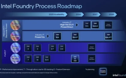
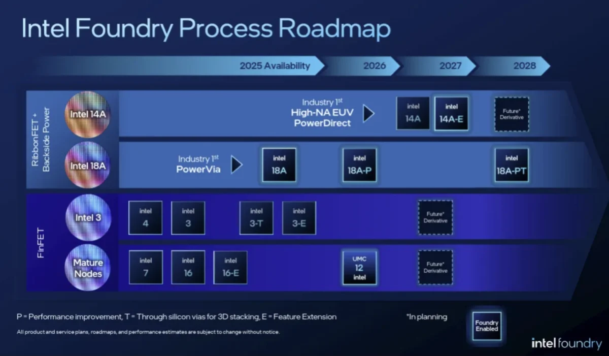
The Intel 14A process is the centerpiece of the company’s long-term manufacturing roadmap. Representing a significant leap forward in transistor architecture and lithographic precision, the 14A node is intended to serve as the foundation for the most demanding workloads of the late 2020s.
The release of PDK version 0.9 is not merely a software update; it is a critical "gate" in the semiconductor development lifecycle. A Process Design Kit acts as the bridge between the foundry’s manufacturing capabilities and the design houses that create the chips. It contains the essential data, design rules, and electrical models that allow engineers to simulate how their circuits will behave on the physical silicon.
Intel has confirmed that the 14A node is currently hitting performance and yield maturity targets consistent with its internal developmental timeline. Crucially, these metrics are not just theoretical; Intel reports that they are backed by actual silicon validation. This means that test wafers have been produced and measured, proving that the manufacturing processes involved—which include advanced Extreme Ultraviolet (EUV) lithography—are functioning within expected parameters.
Chronology: The Path to 14A Readiness
Intel’s transition to the 14A node is the culmination of years of R&D investment and a strategic pivot in the company’s business model. To understand the gravity of the 0.9 PDK release, one must look at the timeline of the foundry’s evolution:
- 2021-2022 (The "Five Nodes" Launch): Under CEO Pat Gelsinger, Intel launched its "IDM 2.0" strategy, promising a rapid cadence of process node transitions, including Intel 7, 4, 3, 20A, and 18A.
- 2023 (The Introduction of 14A): Intel formally unveiled the 14A node during its "Intel Foundry Direct Connect" event. The node was positioned as the successor to 18A, promising significant gains in power efficiency and transistor density.
- Early 2024 (Silicon Validation): Intel began aggressive risk production and test runs to validate the electrical characteristics of the new transistor structures.
- Late 2024 (PDK 0.9 Release): The current milestone. With version 0.9 now in the hands of key partners, the industry enters the "pre-production" phase.
- Q1 2027 (PDK 1.0 Milestone): Intel has scheduled the release of PDK 1.0 for the first quarter of 2027. This version will serve as the "gold" release, signifying that the process is fully qualified for high-volume manufacturing (HVM).
Supporting Data: Understanding the Physics of 14A
The Intel 14A node is built upon the lessons learned from the company’s shift to RibbonFET (Gate-All-Around transistor architecture) and PowerVia (backside power delivery).
Transistor Density and Power Efficiency
While specific density metrics for 14A are proprietary, industry analysts estimate that 14A will offer a double-digit percentage improvement in performance-per-watt over the 18A node. This is achieved by further refining the fin-pitch and metal-pitch dimensions, allowing for a tighter packing of logic gates.
EUV and High-NA Lithography
A critical component of the 14A node is the integration of High-NA (High Numerical Aperture) EUV lithography. Intel has been the industry leader in deploying ASML’s latest-generation High-NA machines. These machines use a larger numerical aperture to project patterns with greater resolution, which is essential for printing the incredibly small features required by the 14A process. The fact that Intel is achieving yield maturity at this stage suggests that their integration of these complex optical systems is successfully maturing.
Silicon Validation Results
The "silicon validation" mentioned by Intel refers to the production of "shuttle" wafers—test chips that contain a variety of standard cell libraries, memory structures, and interconnect test patterns. By measuring these, Intel can verify that the physical manufacturing matches the computer-aided design (CAD) models. The reported maturity indicates that the "defect density"—the number of errors per square centimeter—is currently on a downward trajectory that aligns with the requirements for commercial-scale production.
Official Responses and Industry Context
Intel Foundry has maintained a measured but optimistic tone regarding the 14A rollout. In recent technical briefings, company leadership emphasized that the 14A node is designed to be a "long-lived" node, similar to how 14nm served as the workhorse for the industry for several years.
"Our goal with 14A is to provide a platform that balances cutting-edge performance with the economic viability required by our foundry customers," an Intel spokesperson stated. "By hitting our maturity milestones on schedule, we are proving that our foundry model is not just a concept, but a competitive reality that can support the most sophisticated AI hardware on the planet."
From the perspective of industry analysts, the 14A node represents Intel’s primary opportunity to regain the "process lead" from competitors like TSMC and Samsung. By standardizing the 14A PDK, Intel is attempting to lower the barrier to entry for fabless semiconductor companies—like NVIDIA, AMD, or Qualcomm—to use their manufacturing services. If these companies can trust that the PDK will lead to a predictable, high-yielding product, Intel Foundry will successfully transform from an internal manufacturing arm into a global third-party supplier.
Implications: What This Means for the Future
The release of PDK 0.9 carries profound implications for the semiconductor landscape.
1. The AI Hardware Race
As the demand for AI accelerators grows exponentially, the ability to manufacture chips at smaller, more efficient nodes becomes a bottleneck. The 14A node is specifically optimized for the high-bandwidth, high-current environments required by modern AI GPUs and NPUs. A successful 14A rollout by 2027 ensures that the next generation of generative AI models will have the hardware infrastructure required to scale.
2. Diversifying the Supply Chain
Global supply chain stability has become a paramount concern for governments and corporations alike. By ramping up 14A capacity, Intel is providing an alternative to the heavy concentration of chip manufacturing in East Asia. This is a critical factor for the U.S. and European defense and tech sectors, which are increasingly incentivized to move production to domestic foundries.
3. The Test of Intel’s Foundry Model
This is a "make or break" period for Intel Foundry. The transition to a "foundry-first" mentality requires the company to treat external customers with the same priority as its internal product divisions. The PDK 0.9 release is a signal to these customers that Intel is ready to share the "keys to the kingdom"—the proprietary design rules that define their most advanced manufacturing capabilities.
4. Long-Term Economic Impact
Should Intel hit the Q1 2027 target for PDK 1.0, it will likely trigger a massive capital expenditure cycle across the industry. Companies will begin shifting their long-term design roadmaps toward the 14A process. If Intel maintains this momentum, it could reclaim a significant portion of the foundry market share that it ceded over the last decade.
Conclusion
The release of the Intel 14A PDK version 0.9 is more than just a routine update; it is a testament to the technical progress of a company currently undergoing a massive structural transformation. While the path to 2027 remains fraught with the typical engineering challenges of shrinking features to the atomic level, the progress reported by Intel provides a strong foundation for future optimism. As silicon validation continues and the industry looks toward the 1.0 release, the 14A node stands as a critical checkpoint in the ongoing quest to define the next era of high-performance computing. For investors, engineers, and tech enthusiasts alike, the coming months will be crucial as the industry watches to see if Intel can maintain this pace on the road to full-scale high-volume manufacturing.