
Intel has officially marked a significant milestone in its foundry roadmap, announcing that its "18A-P" (Performance) process node has entered the risk production phase. Revealed in greater technical detail during the VLSI 2026 symposium, this optimized iteration of the company’s 18A process represents a critical pivot in Intel’s strategy to regain manufacturing leadership. By refining its existing architecture rather than forcing a total overhaul, Intel aims to provide a more stable, high-performance pathway for its next generation of data center and consumer products, including the Panther Lake architecture and the robust Xeon 6+ series.
Main Facts: What is 18A-P?
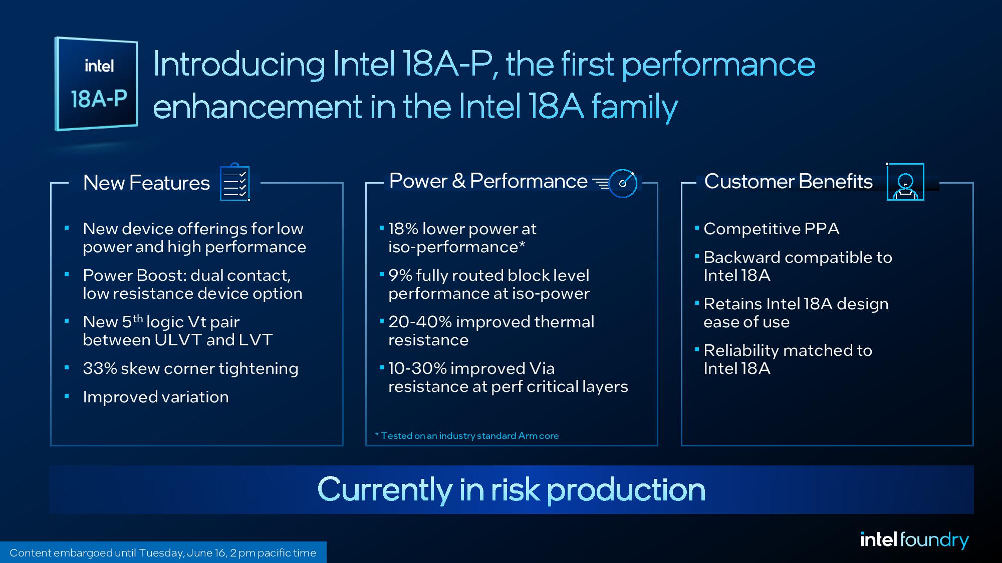
At its core, 18A-P is a performance-optimized derivative of the base 18A process. It is designed to offer a balanced trade-off between power efficiency and raw frequency, boasting a 9% performance increase at equivalent power levels, or, conversely, an 18% reduction in power consumption when maintaining a consistent performance baseline.
The most vital takeaway for industry designers is the process’s backward compatibility. Intel has engineered 18A-P to reside within the same design libraries as the original 18A node, specifically maintaining cell heights of 180nm (High Performance) and 160nm (High Density). This allows existing 18A designs to be ported over to 18A-P without requiring a ground-up redesign. This move is calculated to reduce time-to-market for chip designers who want to capitalize on the performance gains of the "P" iteration without the massive engineering overhead of a full architectural migration.
Chronology: The Road to Risk Production
The development of the 18A-P node did not happen in a vacuum. It follows a series of papers published earlier this year that hinted at the architectural refinements Intel was exploring to improve thermal conductivity and power efficiency.

- Initial Research (Early 2026): Intel began disclosing preliminary findings regarding thermal improvements and signal path optimization.
- VLSI 2026 Disclosure: The official unveiling of the 18A-P technical specifications, detailing the new transistor libraries and threshold voltage options.
- Risk Production (Present Day): Intel has initiated "risk production," a critical stage in semiconductor manufacturing. Unlike high-volume manufacturing (HVM), risk production involves limited-scope wafer output on standard production lines. This allows Intel to gather granular data on defect rates, yield variability, and performance metrics.
Typically, risk production precedes mass volume production by 12 to 24 months. However, because 18A-P is an incremental evolution rather than a leap into an entirely new node (like 14A or beyond), industry experts expect the transition to full-scale production to be significantly faster, potentially condensing the timeline as Intel optimizes its existing 18A-equipped fabs.
Supporting Data: Transistors and Power Efficiency
The technical core of 18A-P lies in its expanded library of transistor designs. Intel has introduced three distinct transistor types, each serving a specific role in the power-performance spectrum:
1. The W3P "Power Boost" Transistor
The W3P design is arguably the most innovative addition. By utilizing a dual-contact structure—with connections on both the front and back sides of the wafer—Intel has significantly reduced parasitic resistance. This structural change allows for a higher drive current, which directly translates to faster switching speeds. When combined with "PowerVia," Intel’s signature backside power delivery technology, the W3P transistor minimizes thermal resistance, effectively creating a more efficient pathway for electricity to reach the transistor gate.
2. Narrow Designs (W1 and W1.5)
To address the "power-optimized" side of the equation, Intel has expanded the availability of its narrow transistor designs. The W1 design, previously exclusive to the 160nm cell library, is now available in the 180nm library. Simultaneously, the W1.5 design is being integrated into the 160nm library. These narrow transistors are specifically tuned for low-power operation, helping designers fill gaps where energy efficiency is more critical than peak clock speed.

3. New Threshold Voltage (VT) Options
Intel is also introducing a new threshold voltage pair: ULVTLL (Ultra-Low Voltage Threshold Low Leakage). To understand its significance, one must look at the standard hierarchy of VT pairs:
- ULVT (Ultra-Low): High performance, high leakage.
- LVT (Low): Balanced performance and leakage.
- SVT (Standard): Baseline for general logic.
- HVT (High): Low performance, very low leakage.
The new ULVTLL slot provides a "Goldilocks" zone—better performance than the standard LVT, but with lower leakage than the aggressive ULVT. This offers designers unprecedented granularity in balancing the power envelopes of complex SoCs.
Official Responses and Strategic Implications
Intel’s executive leadership has remained vocal about the importance of 18A-P, especially in the wake of public scrutiny regarding 18A yields. While the company has acknowledged challenges in the early stages of the 18A rollout, the move to 18A-P is a direct response to customer feedback and the need for higher yields.
Intel has cited a 20% to 40% improvement in thermal resistance and a 10% to 30% reduction in via resistance at "performance-critical" layers. These gains are achieved through advanced EDA (Electronic Design Automation) tools that allow for more precise wafer thinning, ultimately improving the overall heat dissipation of the chips.
The Competitive Landscape
The implications of this shift are profound for the foundry market. Intel is currently ramping up two major U.S.-based fabs to handle 18A production. Despite reports of initial yield struggles, the company remains the primary candidate for several massive high-performance computing (HPC) contracts. Reports suggest that industry giants such as Apple and Nvidia are in ongoing discussions with Intel regarding potential production on the 18A process.
For these external customers, the promise of a "P" revision is highly attractive. It suggests that Intel is not only capable of mass-producing advanced nodes but is actively iterating to ensure those nodes remain competitive against rivals like TSMC. If Intel can successfully demonstrate that 18A-P delivers consistent yields, it will go a long way toward rebuilding market confidence.
Conclusion: A Pivot Toward Stability
The introduction of 18A-P signifies a mature approach to semiconductor manufacturing. Rather than chasing the headlines of a "next-generation" number, Intel is focusing on the "how" of manufacturing—improving thermal conductivity, reducing resistance, and providing designers with more flexible building blocks.
As the industry moves toward 2027 and 2028, the success of 18A-P will likely be the barometer by which Intel Foundry’s viability is judged. If the company can prove that these incremental gains, combined with the power of its U.S. fabrication capacity, can meet the rigorous demands of AI-focused silicon providers, the 18A-P node could be remembered as the turning point where Intel reclaimed its manufacturing edge.
For the average consumer, this means that upcoming generations of processors—starting with the Panther Lake line—will likely benefit from better thermal management and improved efficiency, directly addressing the common concerns of power consumption and heat in high-end computing. Intel is not just betting on the future; they are effectively re-engineering the present to ensure that their current silicon roadmap remains robust, competitive, and, above all, manufacturable.