In the high-stakes world of semiconductor manufacturing, even the industry’s undisputed titan is not immune to the laws of physics. Nvidia, the architect of the AI revolution, is currently navigating a significant strategic pivot regarding its upcoming "Rubin Ultra" platform. After months of speculation, industry reports now confirm that the originally envisioned 4-tile version of the Rubin Ultra chip has been scrapped. The culprit? Severe packaging limitations that rendered the massive, multi-die architecture commercially unviable.
This development marks a critical inflection point for Nvidia, which has relied on monolithic-style performance to maintain its dominance. As manufacturing yields for ultra-large chips collapse under the pressure of physical deformation, the company is being forced to reconsider its roadmap, opening a narrow window of opportunity for competitors like AMD to close the gap.
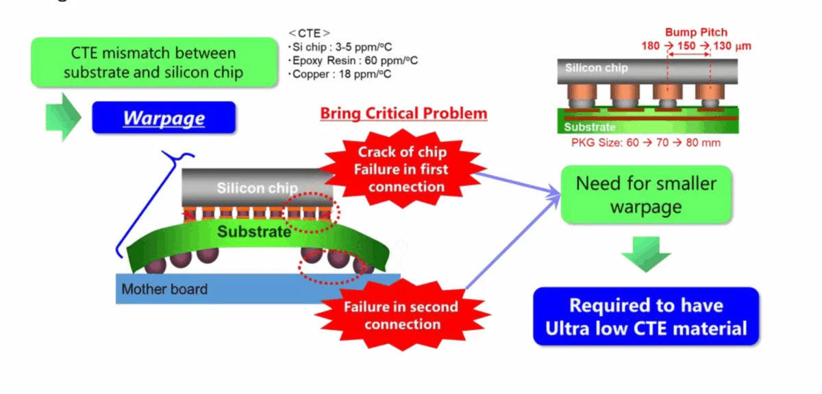
The Core Problem: The Physics of "Warpage"
At the heart of the failure lies a phenomenon known as "warpage." As semiconductor manufacturers push the boundaries of what is possible, they have moved toward "chiplets"—combining multiple smaller silicon tiles onto a single package to create a "super-chip."
When these tiles are assembled, they are bonded to a substrate. However, the materials involved—silicon, copper, and organic substrates—all expand and contract at different rates when subjected to the intense heat of the manufacturing process. In the case of the 4-tile Rubin Ultra, the sheer surface area of the chip caused the package to warp during cooling. This deformation is not merely cosmetic; it creates micro-fractures in the delicate interconnections, causing the chip to fail electrical testing.
According to analysis from SemiAnalysis, Nvidia attempted multiple engineering workarounds, including a "native" 4-tile design and a modular "2+2" architecture. Neither approach yielded a high enough percentage of functional chips to justify mass production. The "yield" problem—the ratio of perfect chips to defective ones on a single silicon wafer—dropped to unacceptable levels, rendering the 4-tile design a manufacturing impossibility for the current state of TSMC’s CoWoS-L (Chip-on-Wafer-on-Substrate) packaging technology.
Chronology of a Strategic Pivot
The path to this realization has been paved with industry skepticism and internal re-evaluations.
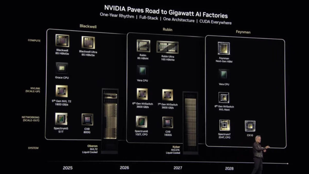
- March 2024: Initial reports began to circulate regarding the ambitious design of the Rubin Ultra. Analysts noted that the chip was pushing the theoretical limits of TSMC’s CoWoS-L packaging capacity.
- Late Spring 2024: Internal test runs confirmed that warpage was occurring at a rate that made large-scale production impossible. The "4-tile" dream became a technical bottleneck.
- Summer 2024: Nvidia officially signaled a change in direction. The company moved to abandon the 4-tile design entirely, pivoting to a revised Rubin Ultra architecture that relies on a single 2-tile configuration, supplemented by faster memory and higher clock speeds to compensate for the reduction in die count.
- Current Status: Nvidia is currently recalibrating its supply chain to prioritize the 2-tile variant, aiming to maintain performance gains through architectural optimization rather than sheer physical size.
Implications: The Eroding CUDA Moat
For years, Nvidia’s primary defense against competition was not just its hardware, but the "CUDA moat"—a massive ecosystem of software libraries that made Nvidia hardware the only logical choice for AI researchers. However, the technical struggles with Rubin Ultra coincide with a period where that moat is showing signs of evaporation.
Large cloud service providers (CSPs) like Google, Amazon, and Microsoft—the primary customers for Nvidia’s GPUs—are increasingly investing in their own internal silicon. Google’s TPUs and Amazon’s Trainium chips are no longer niche curiosities; they are powering the next generation of AI agents.
SemiAnalysis recently noted that a significant portion of inference tasks for advanced AI models, such as Claude Code, is now being shifted to internal hardware like Trainium. A year ago, this level of diversification was unthinkable. The industry is witnessing a decoupling of AI software from Nvidia’s proprietary hardware, a shift that makes any manufacturing delay at Nvidia significantly more dangerous for their long-term market share.

Can AMD Capitalize on the Packaging Gap?
While Nvidia grapples with the physical limits of its current packaging, its rival AMD is arguably in a better position to exploit the situation. AMD has been a pioneer in chiplet-based designs for years, leveraging TSMC’s advanced packaging technologies with great success.
The upcoming Instinct MI455X and the projected MI500 series are being watched closely. While Nvidia is reportedly looking toward its "Feynman" generation in 2028 to solve its packaging issues through advanced 3D stacking (SoIC), AMD is already utilizing these technologies in its current product lines.
The move to 3D stacking is the "Holy Grail" of modern chip design. By stacking silicon dies vertically rather than spreading them horizontally across a wide substrate, engineers can reduce the footprint and minimize the thermal stresses that cause warpage. Reports suggest that AMD’s MI450 already utilizes a sophisticated 4-die stack (four XCDs) on two base dies, proving that the technology is not only viable but ready for deployment.
The Road Ahead: Materials and Future Tech
Nvidia is not standing still, but the path to recovery is paved with expensive R&D. The industry is currently in a race to move beyond traditional organic substrates.
The Shift to Glass Substrates
One of the most promising avenues for future AI chips is the transition to glass substrates. Unlike organic materials, glass offers superior mechanical stability and flatness, which would effectively eliminate the warpage issues currently plaguing the Rubin Ultra. However, integrating glass into mass-market manufacturing is a multi-year challenge. Samsung and other leaders in the space are targeting 2028 for the widespread adoption of glass-substrate technology.
The Role of TSMC
TSMC remains the arbiter of this war. Their "SoIC" (System-on-Integrated-Chips) and "X3D" stacking technologies are the primary enablers of the next decade of compute. While Nvidia and AMD fight for capacity, TSMC’s ability to refine these packaging techniques will dictate which company wins the AI hardware race. If Nvidia can successfully integrate 3D stacking into the Feynman platform, they may well regain their lead. But until then, the company is fighting a war on two fronts: one against competitors who are finally learning to build chips as well as they do, and one against the fundamental physics of silicon itself.
Conclusion: A Humbling Lesson in Scale
The cancellation of the 4-tile Rubin Ultra is a sobering reminder that in the semiconductor industry, bigger is not always better. Nvidia’s attempt to brute-force performance through massive die counts hit a wall that money and market dominance could not break.
The industry is now entering an era of "intelligent efficiency." Moving forward, the winners will not necessarily be those with the largest chips, but those who can most effectively manage the complex interplay of power, heat, and structural integrity. Nvidia remains the dominant force in the AI ecosystem, but the path forward is no longer a straight line—it is a complex, multi-layered puzzle that requires as much innovation in packaging as it does in GPU architecture. For the market, this period of struggle is a sign of a maturing industry, one where the "moat" is no longer enough to keep the competition at bay.